AD7228KR Просмотр технического описания (PDF) - Analog Devices
Номер в каталоге
Компоненты Описание
производитель
AD7228KR Datasheet PDF : 15 Pages
| |||
Data Sheet
Timing Deskew
Signal edges slowing or rounding off by the time they reach the
pin driver circuitry is a common problem in automated test
equipment (ATE) applications. Square up the edge at the pin
driver to overcome this problem. However, because each edge is
not rounded off by the same extent, this squaring up may lead
to incorrect timing relationship between signals. This effect is
shown in Figure 13.
BUFFER TRIGGER POINT
HIGH-SPEED
BUFFER
Figure 13. Time Skewing Due to Slowing of Edges
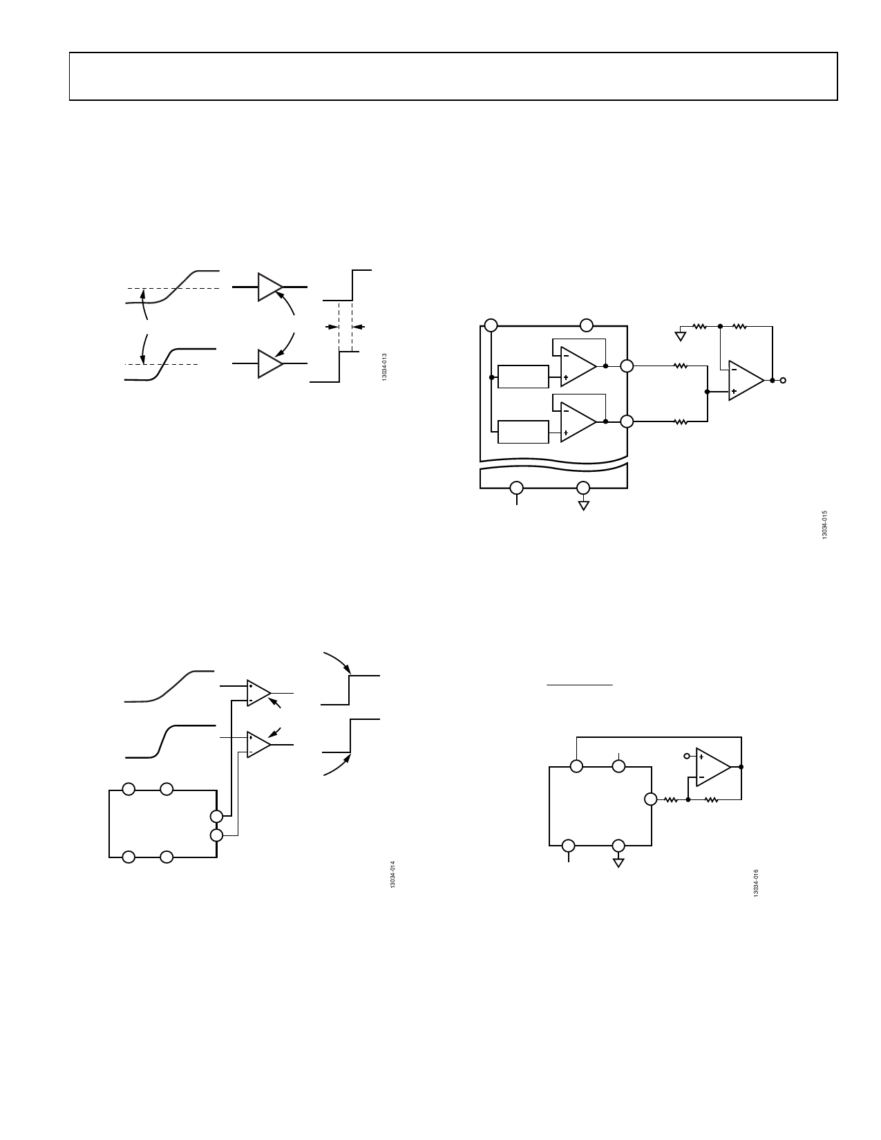
The circuit of Figure 14 shows how two DACs of the AD7228
can help overcome the problem of time skewing. The same two
signals are applied to this circuit as are applied in Figure 14. The
output of each DAC is applied to one input of a high speed
comparator, and the signals are applied to the other inputs.
Varying the output voltage of the DAC effectively varies the
trigger point at which the comparator flips. Therefore, the timing
relationship between the two signals can be programmably
corrected (or deskewed) by varying the code to the DAC of
the AD7228. In a typical application, the code is loaded to the
DACs for correct timing relationships during the calibration
cycle of the instrument.
POSITION OF THIS EDGE
PROGRAMMED BY CODE
TO DAC1
HIGH-SPEED
COMPARATORS
11
VREF
1
VDD
AD7228* VOUT1 9
VSS
GND VOUT2 8
10
12
POSITION OF THIS EDGE
PROGRAMMED BY CODE
TO DAC2
*ADDITIONAL PINS OMITTED FOR CLARITY.
Figure 14. AD7228 Timing Deskew Circuit
Coarse/Fine Adjust
Pair the DACs on the AD7228 together to form a coarse/fine
adjust function as shown in Figure 15. The function is achieved
using one external op amp and a few resistors per pair of DACs.
AD7228
DAC 1 is the most significant or coarse DAC. Data is first loaded to
this DAC to coarsely set the output voltage. DAC 2 is then used
to fine tune this output voltage. Varying the ratio of R1 to R2
varies the relative effect of the coarse and fine DACs on the
output voltage. For the resistor values shown, DAC 2 has a
resolution of 150 μV in a 10 V output range. Because each DAC
on the AD7228 is guaranteed monotonic, the coarse adjustment
and fine adjustment are each monotonic. One application for
this is as a setpoint controller (see the AN-317 Application
Note, “Circuit Applications of the AD7226 Quad CMOS DAC,”
available from Analog Devices, Inc.).
VREF
11
VDD
1
51.2kΩ 200Ω
DAC 1
VOUT1 200Ω
9
A1
VOUT
DAC 2
VOUT2 51.2kΩ
8
AD7228*
10
VSS
–5V
12
GND
*ADDITIONAL PINS OMITTED FOR CLARITY.
Figure 15. Coarse/Fine Adjust Circuit
Self Programmable Reference
The circuit of Figure 16 shows how one DAC of the AD7228, in
this case DAC 1, can be used in a feedback configuration to
provide a programmable reference for itself and the other seven
converters. The relationship of VREF to VIN is expressed by
VREF
(1 G)
(1 G D1)
VIN
where G = R2/R1.
11
VREF
+15V
1
VDD
VIN
A1
AD7228* VOUT1 9 R1
R2
VSS
GND
10
12
–5V
*ADDITIONAL PINS OMITTED FOR CLARITY.
Figure 16. Self Programmable Reference
Rev. D | Page 11 of 15
Share Link: 