SPT2110 Просмотр технического описания (PDF) - Signal Processing Technologies
Номер в каталоге
Компоненты Описание
производитель
SPT2110 Datasheet PDF : 20 Pages
| |||
The following assumes the address register is already set.
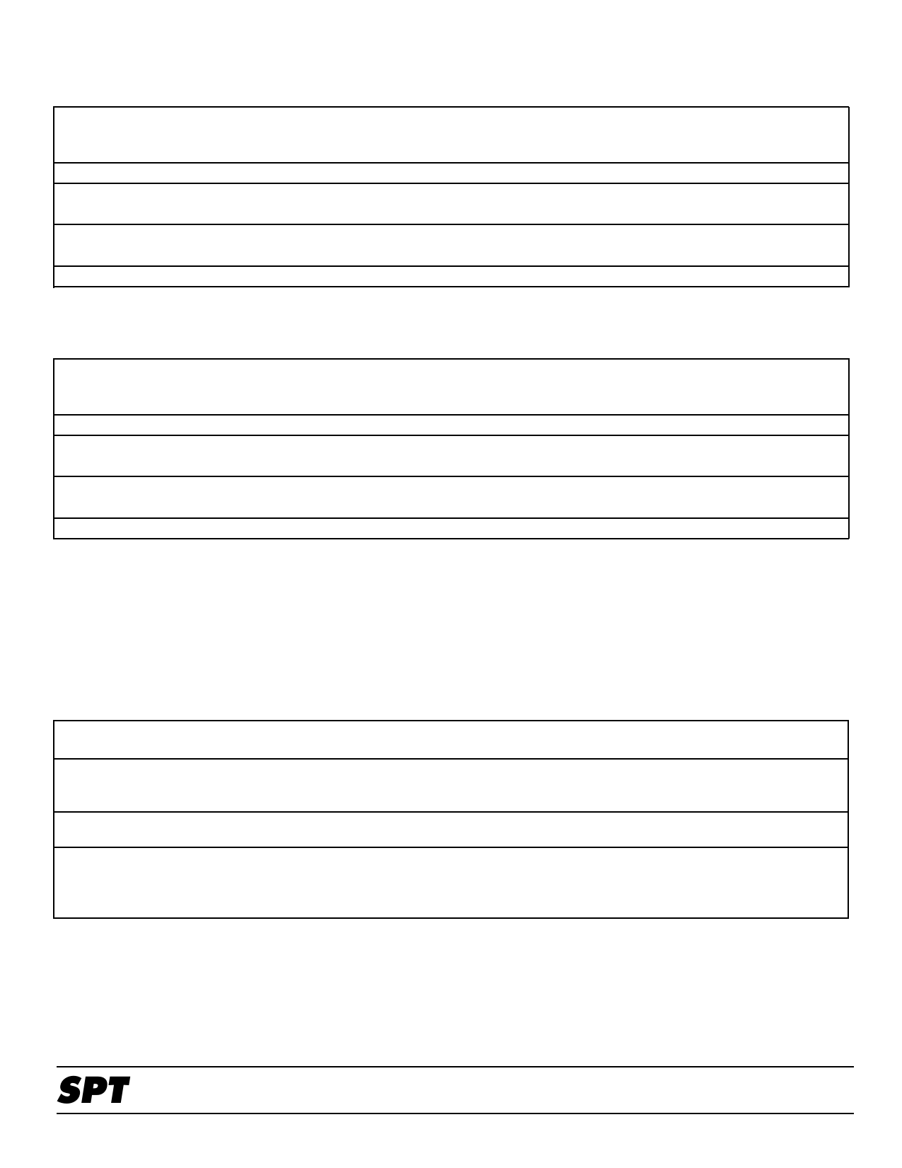
Table VIII - Write Command Register
CONT.
STATE\
STEP
1
CS_ WR_ RD_ RS
0
1
1
1
2
0
0
1
1
3
0
1
1
1
4
1
1
1
X
Data (7-0)
DDh
DDh
DDh
XXh
Comments
Data needs to be valid on the data bus for minimum setup time
(relative to the WR_ signal).
Data needs to remain valid on the data bus for minimum hold
time (relative to the WR_ signal).
Completed Command Write.
Table IX - Read Command Register
CONT.
STATE\
STEP
CS_ WR_ RD_ RS
1
0
1
1
1
2
0
1
0
1
3
0
1
1
1
4
1
1
1
X
Data (7-0)
XXh
DDh
XXh
XXh
Comments
Data is valid on the data bus after output delay time (relative to
the RD_ signal).
Data continues to remain valid for output hold time delay (relative
to the RD_ signal).
Completed Command Read.
If the address already contains the correct address of the register to be accessed, it is not necessary to perform
an address register write. Only a command register acquisition is required to write or read the command register.
OTHER DISCRETE SIGNALS
The other signals not discussed are the Reset, Status and OE signals. The following table describes these functions.
Table X - Other Discrete Signals
Signal
Name
RESET_
Input/
Output
INPUT
STATUS_ OUTPUT
OE_
INPUT
Description
This signal is an input active low. It requires three or more input clocks while the signal
is active to reset the device. It resets all registers to their default states and clears all
data within the device.
This signal is an output active low signal. It will be asserted whenever video sync is
being detected and will go inactive when sync is not detected.
When asserted, this signal enables the output signals. This is an active low logic signal.
It tri-states the outputs when deasserted and enables them when asserted. The signals
that are controlled are the data output busses (RGB/YC), HSYNC, VSYNC, HBLNK,
VBLNK, ODD and CFLAG.
SPT
5
SPT2110
3/27/98
Share Link: 