SPT2110 Просмотр технического описания (PDF) - Signal Processing Technologies
Номер в каталоге
Компоненты Описание
производитель
SPT2110 Datasheet PDF : 20 Pages
| |||
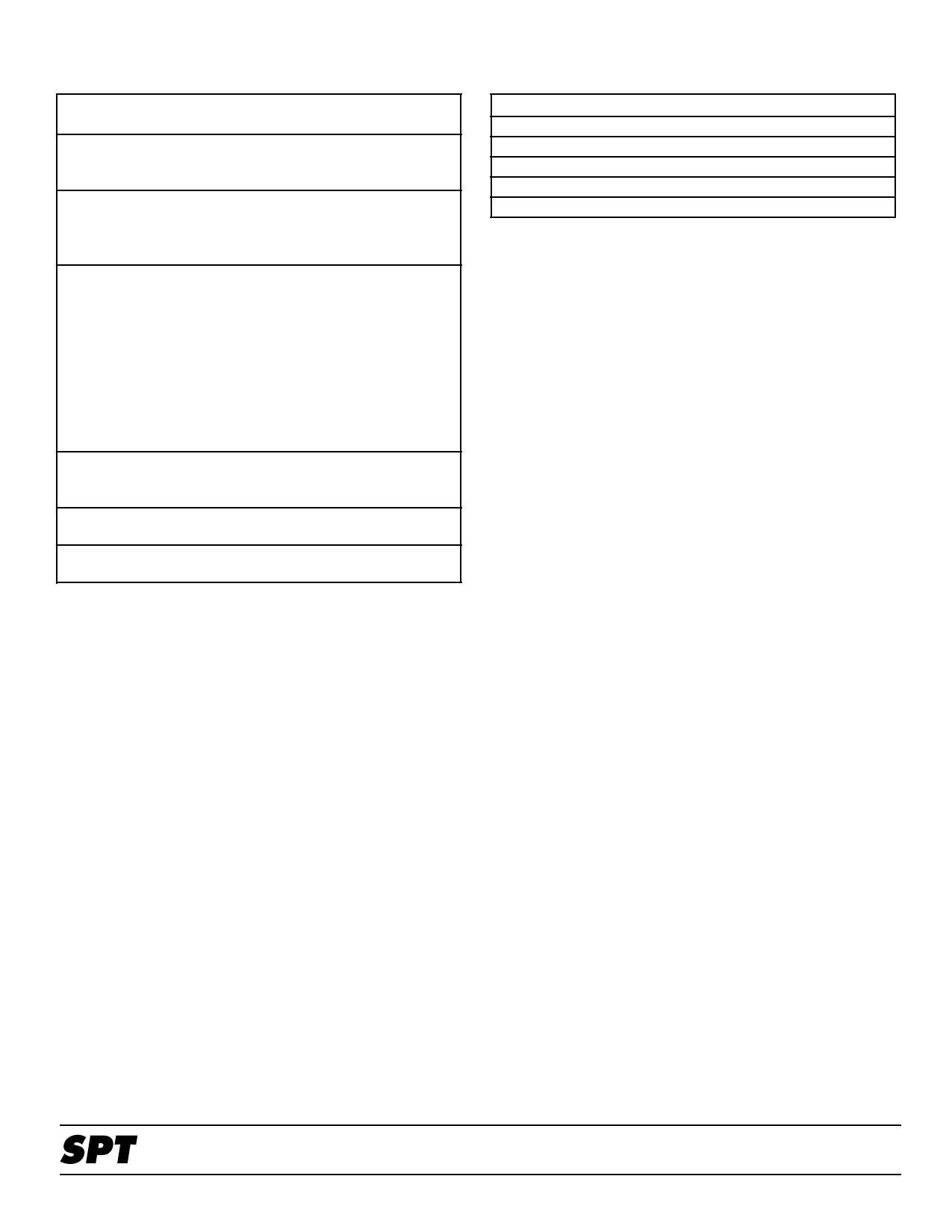
Table III - Timing Control Signal Description
Table IV - Sample Mode Clock Frequencies
Signal
Label Description
HSYNC This is the horizontal synchronizing signal; its
width is equal to the width of the incoming
digitized video signal.
VSYNC This is the vertical synchronizing signal. 3H time
for NTSC starting after the three H lines of
equalizing pulses and 2.5H time for PAL starting
at beginning of line 1 and line 312.5.
HBLNK This is the horizontal blanking signal. Registers
DH and EH control the start and stop locations
of the active pixels. When this signal is
deasserted the following number of active video
pixels is displayed for the various sampling
modes.
- ITU-R BT.601
720 active pixels
- NTSC square pixel 640 active pixels
- NTSC4Fsc
768 active pixels
- PAL square pixel 768 active pixels
VBLNK This is the vertical blanking signal. Registers FH
and 10H control the start and stop locations of
the active lines.
ODD When active, this signal indicates that the odd
field is being output from the decoder.
CFLAG This signal indicates whether Cb or Cr data is
active.
Note: Due to asynchronous sampling of the video signal, a
periodic deviation of the sync width by one pixel clock may
be generated in HSYNC, VSYNC, HBLNK, VBLNK and
ODD signals.
CLOCK SIGNAL
The clock (CLK) input has is 3.3 volt compatible logic. The
clock is the master time-base controller for the SPT2110. The
SPT2110 synchronizes data input, data output, control signal
out, address and command register modifications and data
processing to the clock. A stable, jitter-free clock signal
should be used.
Sampling Mode
NTSC Square Pixel
NTSC ITU-R (CCIR-601)
NTSC 4 Fsc
PAL Square Pixel
PAL ITU-R (CCIR-601)
Input Frequency (MHz)
12.2727
13.500
14.3182
14.7500
13.5000
MPU INTERFACE
The SPT2110 provides for microprocessor unit (MPU) based
programming and control through a 3.3 V compatible logic
interface. The MPU interface is comprised of a bidirectional
8-bit data bus and four discrete control registers. A descrip-
tion of this interface is shown in table V.
COMMAND AND ADDRESS REGISTERS
The SPT2110 operational performance is controlled by inter-
nal command registers that are accessed through the MPU
interface described above. There is one address register and
20 command registers (0H - 13H). All registers have read/
write capability.
The address register is used to identify the command register
to be operated. This register must be written to first with the
address of the target command register before a read/write
operation can be performed on the command register. Tables
VI and VII describe the normal operation for reading and
writing to the address register.
Most of the command registers control multiple functions, i.e.,
each bit or group of bits within a register controls a chip
function. When modifying a register a read of the register
should be performed first. Then alter the bit(s) while maintain-
ing the rest of the bits in their present state. Finally, write the
modified data back into the register.
Tables VIII and IX describe the operation for reading and
writing to a selected command register. All registers have a
default setting when the STP2110 is reset. For a detailed
description of the functions of each register, refer to table XIII,
Command Register Description Table.
SPT
3
SPT2110
3/27/98
Share Link: 