ADR291FR-REEL Просмотр технического описания (PDF) - Analog Devices
Номер в каталоге
Компоненты Описание
производитель
ADR291FR-REEL Datasheet PDF : 15 Pages
| |||
ADR290/ADR291/ADR292
an additional operational amplifier is not required for either
reinversion (current-switching mode) or amplification (voltage-
switching mode) of the DAC output voltage. In general, any
positive voltage reference can be converted into a negative volt-
age reference through the use of an operational amplifier and a
pair of matched resistors in an inverting configuration. The dis-
advantage to that approach is that the largest single source of
error in the circuit is the relative matching of the resistors used.
The circuit illustrated in Figure 32 avoids the need for tightly
matched resistors with the use of an active integrator circuit. In
this circuit, the output of the voltage reference provides the
input drive for the integrator. The integrator, to maintain circuit
equilibrium adjusts its output to establish the proper relationship
between the reference’s VOUT and GND. Thus, any negative
output voltage desired can be chosen by simply substituting for
the appropriate reference IC. One caveat with this approach
should be mentioned: although rail-to-rail output amplifiers
work best in the application, these operational amplifiers require
a finite amount (mV) of headroom when required to provide
any load current. The choice for the circuit’s negative supply
should take this issue into account.
VIN
2
ADR29x 6
VOUT
GND
4
100k⍀
1k⍀
1F
1F
+5V
A1
–5V
100⍀
–VREF
A1 = 1/2 OP291,
1/2 OP295
Figure 32. A Negative Precision Voltage Reference Uses
No Precision Resistors
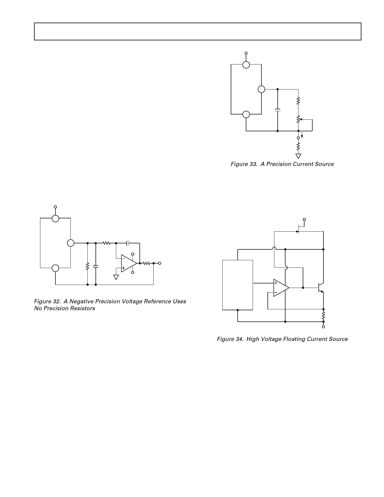
A Precision Current Source
Many times in low power applications, the need arises for a pre-
cision current source that can operate on low supply voltages.
As shown in Figure 33, any one of the devices in the ADR29x
family of references can be configured as a precision current
source. The circuit configuration illustrated is a floating current
source with a grounded load. The reference’s output voltage is
bootstrapped across RSET, which sets the output current into the
load. With this configuration, circuit precision is maintained for
load currents in the range from the reference’s supply current,
typically 12 µA to approximately 5 mA.
VIN
2
ADR29x 6
VOUT
GND
4
1F
ISY
ADJUST
·R1
RSET
P1
IOUT
RL
Figure 33. A Precision Current Source
High Voltage Floating Current Source
The circuit of Figure 34 can be used to generate a floating cur-
rent source with minimal self heating. This particular configura-
tion can operate on high supply voltages determined by the
breakdown voltage of the N-channel JFET.
+VS
E231
SILICONIX
VIN
ADR290
GND
OP90
2N3904
2.10k⍀
–VS
Figure 34. High Voltage Floating Current Source
Kelvin Connections
In many portable instrumentation applications, where PC board
cost and area go hand-in-hand, circuit interconnects are very often
of dimensionally minimum width. These narrow lines can cause
large voltage drops if the voltage reference is required to provide
load currents to various functions. In fact, a circuit’s interconnects
can exhibit a typical line resistance of 0.45 mW/square (1 oz. Cu,
for example). Force and sense connections also referred to as
Kelvin connections, offer a convenient method of eliminating the
effects of voltage drops in circuit wires. Load currents flowing
through wiring resistance produce an error (VERROR = R ϫ IL ) at
the load. However, the Kelvin connection of Figure 35, overcomes
the problem by including the wiring resistance within the forcing
loop of the op amp. Since the op amp senses the load voltage, op
amp loop control forces the output to compensate for the wiring
error and to produce the correct voltage at the load.
REV. A
–13–
Share Link: 