NX25P40-VNI Просмотр технического описания (PDF) - NexFlash -> Winbond Electronics
Номер в каталоге
Компоненты Описание
производитель
NX25P40-VNI
NexFlash -> Winbond Electronics

NX25P40-VNI Datasheet PDF : 28 Pages
| |||
1M / 2M / 4M-BIT SERIAL FLASH MEMORY with 40MHz SPI
NX25P10, NX25P20 AND NX25P40
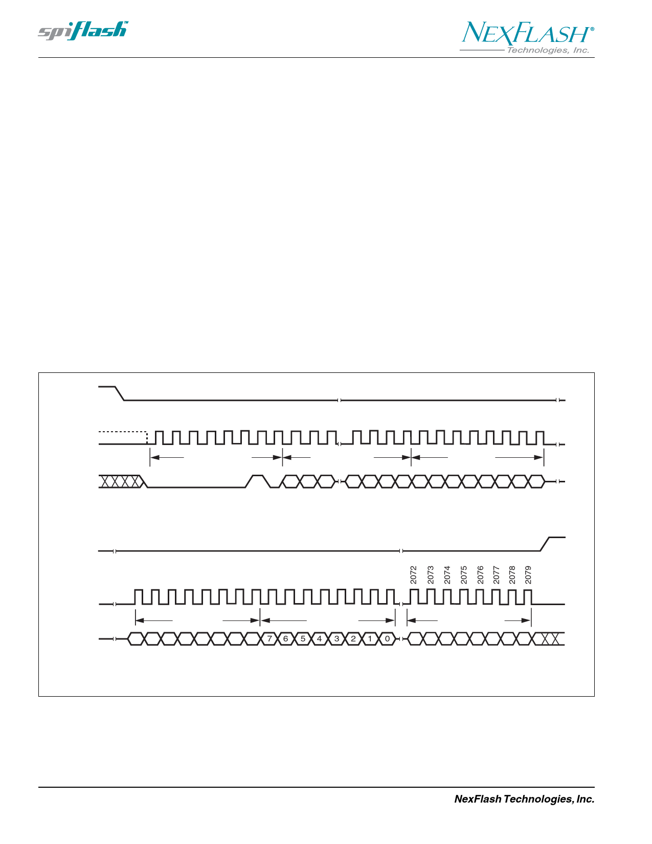
Page Program (02h)
The Page Program instruction allows from one byte to 256
bytes of data to be programmed at memory locations
previously erased to all 1s (FFh). A Write Enable instruction
must be executed before the device will accept the Page
Program Instruction (Status Register bit WEL must equal
1). The instruction is initiated by driving the CS pin low then
shifting the instruction code “02h” followed by a 24-bit
address (A23-A0) and at least one data byte, into the DI pin.
The CS pin must be driven low for the entire length of the
instruction while data is being sent to the device. The Page
Program instruction sequence is shown in figure 10.
If an entire 256 byte page is to be programmed, the last
address byte (the 8 least significant address bits) should be
set to 0. If the last address byte is not zero, and the number
of clocks exceed the remaining page length, the addressing
will wrap to the beginning of the page. Less than 256 bytes
can be programmed without having any effect on other
bytes within the same page. If more than 256 bytes are sent
to the device the addressing will wrap to the beginning of the
page and overwrite previously sent data.
As with the write and erase instructions, the CS pin must be
driven high after the eighth bit of the last byte has been
latched. If this is not done the Page Program instruction will
not be executed. After CS is driven high, the self-timed
Page Program instruction will commence for a time duration
of tpp (See AC Characteristics). While the Page Program
cycle is in progress, the Read Status Register instruction
may still be accessed for checking the status of the BUSY
bit. The BUSY bit is a 1 during the Page Program cycle and
becomes a 0 when the cycle is finished and the device is
ready to accept other instructions again. After the Page
Program cycle has started the Write Enable Latch (WEL) bit
in the Status Register is cleared to 0. The Page Program
instruction will not be executed if the addressed page is
protected by the Block Protect (BP2, BP1, BP0) bits (see
Table 2).
CS
Mode 3
CLK Mode 0
DI
0 1 2 3 4 5 6 7 8 9 10 28 29 30 31 32 33 34 35 36 37 38 39
Instruction (02h)
24-Bit Address
Data Byte 1
23 22 21
*
321 076543210
*
CS
CLK
DI
40 41 42 43 44 45 46 47 48 49 50 51 52 53 54 55
Data Byte 2
Data Byte 3
76 5 4 3 21 0 76 54 321 0
*
*
Data Byte 256
76543210
*
* = MSB
Figure 10. Page Program Instruction Sequence Diagram
16
NexFlash Technologies, Inc.
PRELIMINARY MKP-0009 Rev 6 NXSF040I-0405
04/04/05 ©
Share Link: