LC75810E Просмотр технического описания (PDF) - ON Semiconductor
Номер в каталоге
Компоненты Описание
производитель
LC75810E Datasheet PDF : 54 Pages
| |||
LC75810E/T
• Display on/off control • • • <Turns the display on or off.>
Code
D120 D121 D122 D123 D124 D125 D126 D127 D128 D129 D130 D131 D132 D133 D134 D135 D136 D137 D138 D139 D140 D141 D142 D143
DG1 DG2 DG3 DG4 DG5 DG6 DG7 DG8 DG9
DG1
0
DG1
1
DG1
2
DG1
3
DG1
4
DG1
5
DG1
6
M
A SC BU 0
0
1
0
M, A: Specifies the data to be turned on or off.
MA
Display operating state
0 0 Both MDATA and ADATA are turned off. (The display is forcibly turned off, regardless of the DG1 to DG16 data.)
0 1 Only ADATA is turned on. (The ADATA of display digits specified by the DG1 to DG16 data are turned on.)
1 0 Only MDATA is turned on. (The MDATA of display digits specified by the DG1 to DG16 data are turned on.)
1 1 Both MDATA and ADATA are turned on. (The MDATA and ADATA of display digits specified by the DG1 to DG16 data are turned on.)
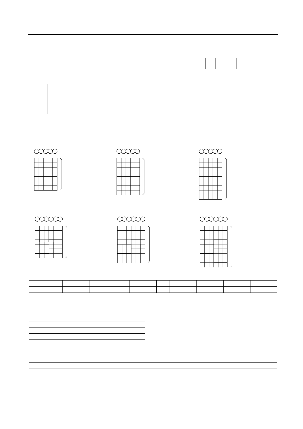
*14: MDATA, ADATA
5 × 7 dot matrix
• • • • • ADATA
5 × 8 dot matrix
• • • • • ADATA
5 × 9 dot matrix
• • • • • ADATA
• • • MDATA
• • • MDATA
• • • MDATA
6 × 7 dot matrix
• • • • • ADATA
• • • MDATA
6 × 8 dot matrix
• • • • • ADATA
• • • MDATA
6 × 9 dot matrix
• • • • • ADATA
• • • MDATA
DG1 to DG16: Specifies the display digit.
Display digit
1
2
3
4
5
6
7
8
9
10
11
12
13
14
15
16
Display digit data DG1 DG2 DG3 DG4 DG5 DG6 DG7 DG8 DG9 DG10 DG11 DG12 DG13 DG14 DG15 DG16
For example, if DG1 to DG8 are 1, and DG9 to DG16 are 0, then display digits 1 to 8 will be turned on, and display digits
9 to 16 will be turned off (blanked).
SC: Controls the common and segment output pins.
SC
Common and segment output pin states
0
Output of LCD drive waveforms
1
Fixed at the VSS level (all segments off)
Note ∗15: When SC is 1, the S1 to S80 and COM1 to COM10 output pins are set to the VSS level, regardless of the M, A, and DG1 to DG16 data.
BU: Controls the normal mode and power saving mode.
BU
Mode
0
Normal mode
Power saving mode
1
(In this mode, the OSC pin oscillator is stopped, and the common and segment pins are set to the VSS level. In this mode, instructions other than
the “display on/off control” and “set display contrast” instructions cannot be executed. Thus applications must set the IC to normal mode before
executing any of the other instructions.)
No.7141-13/54
Share Link: 