ST72324J2-AUTO Просмотр технического описания (PDF) - STMicroelectronics
Номер в каталоге
Компоненты Описание
производитель
ST72324J2-AUTO
STMicroelectronics

ST72324J2-AUTO Datasheet PDF : 194 Pages
| |||
ST72324xx-Auto
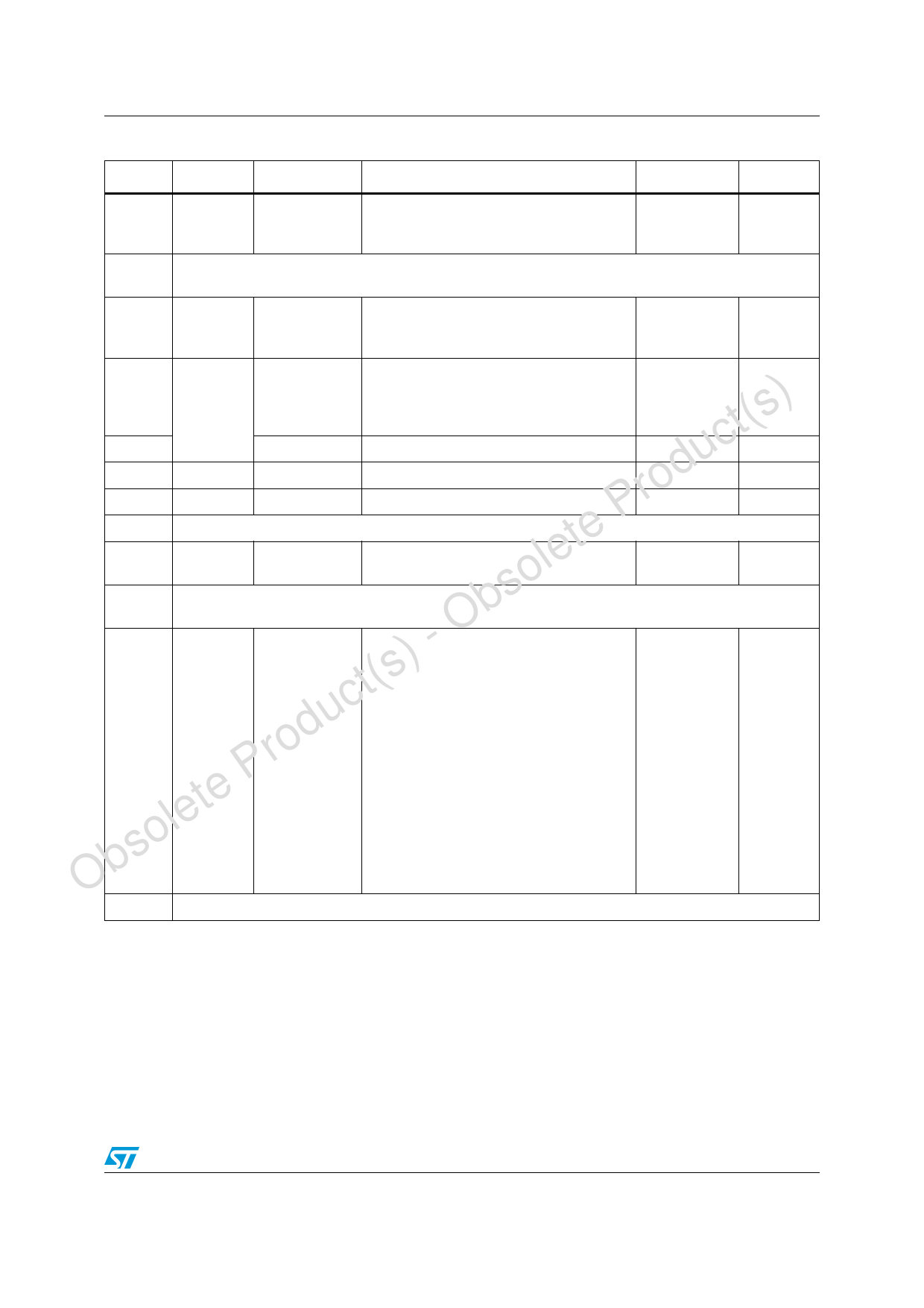
Register and memory map
Table 3. Hardware register map (continued)
Address Block Register label
Register name
Reset status Remarks
000Fh
0010h
0011h
Port F(1)
PFDR
PFDDR
PFOR
Port F data register
Port F data direction register
Port F option register
00h(2)
00h
00h
R/W
R/W
R/W
0012h to
0020h
Reserved area (15 bytes)
0021h
0022h
0023h
SPIDR
SPI SPICR
SPICSR
SPI data I/O register
SPI control register
SPI control/status register
xxh
R/W
0xh
R/W
00h
R/W
0024h
0025h
) 0026h
t(s 0027h
ISPR0
ISPR1
ITC
ISPR2
ISPR3
c 0028h
EICR
du 0029h
Flash FCSR
ro 002Ah Watchdog WDGCR
P 002Bh
te 002Ch
le 002Dh
MCC
MCCSR
MCCBCR
so 002Eh to
b 0030h
O 0031h
- 0032h
t(s) 0033h
0034h
c 0035h
u 0036h
d 0037h
ro 0038h
P 0039h
003Ah
te 003Bh
le 003Ch
o 003Dh
s003Eh
Ob003Fh
Timer A
TACR2
TACR1
TACSR
TAIC1HR
TAIC1LR
TAOC1HR
TAOC1LR
TACHR
TACLR
TAACHR
TAACLR
TAIC2HR
TAIC2LR
TAOC2HR
TAOC2LR
Interrupt software priority register 0
Interrupt software priority register 1
Interrupt software priority register 2
Interrupt software priority register 3
External interrupt control register
Flash control/status register
Watchdog control register
Reserved area (1 byte)
Main clock control/status register
Main clock controller: beep control register
FFh
R/W
FFh
R/W
FFh
R/W
FFh
R/W
00h
R/W
00h
R/W
7Fh
R/W
00h
R/W
00h
R/W
Reserved area (3 bytes)
Timer A control register 2
Timer A control register 1
Timer A control/status register(3)(4)
Timer A input capture 1 high register
Timer A input capture 1 low register
Timer A output compare 1 high register
Timer A output compare 1 low register
Timer A counter high register
Timer A counter low register
Timer A alternate counter high register
Timer A alternate counter low register
Timer A input capture 2 high register(3)
Timer A input capture 2 low register(3)
Timer A output compare 2 high register(4)
Timer A output compare 2 low register(4)
00h
00h
xxxx x0xxb
xxh
xxh
80h
00h
FFh
FCh
FFh
FCh
xxh
xxh
80h
00h
R/W
R/W
R/W
Read only
Read only
R/W
R/W
Read only
Read only
Read only
Read only
Read only
Read only
R/W
R/W
0040h
Reserved area (1 byte)
Doc ID 13841 Rev 1
21/193
Share Link: