KSZ8051MNL Просмотр технического описания (PDF) - Microchip Technology
Номер в каталоге
Компоненты Описание
производитель
KSZ8051MNL Datasheet PDF : 66 Pages
| |||
KSZ8051MNL/RNL
3.3 RMII Data Interface (KSZ8051RNL Only)
The Reduced Media Independent Interface (RMII) specifies a low pin count Media Independent Interface (MII). It pro-
vides a common interface between physical layer and MAC layer devices, and has the following key characteristics:
• Pin count is 8 pins (3 pins for data transmission, 4 pins for data reception, and 1 pin for the 50 MHz reference
clock).
• 10 Mbps and 100 Mbps data rates are supported at both half- and full-duplex.
• Data transmission and reception are independent and belong to separate signal groups.
• Transmit data and receive data are each 2 bits wide, a dibit.
3.3.1 RMII - 25 MHZ CLOCK MODE
The KSZ8051RNL is configured to RMII - 25 MHz clock mode after it is powered up or hardware reset with the following:
• A 25 MHz crystal connected to XI, XO (pins 9, 8), or an external 25 MHz clock source (oscillator) connected to XI.
• The CONFIG[2:0] strap-in pins (pins 18, 29, 28) set to 001.
• Register 1Fh, bit [7] is set to 0 (default value) to select 25 MHz clock mode.
3.3.2 RMII - 50 MHZ CLOCK MODE
The KSZ8051RNL is configured to RMII - 50 MHz clock mode after it is powered up or hardware reset with the following:
• An external 50 MHz clock source (oscillator) connected to XI (pin 9).
• The CONFIG[2:0] strap-in pins (pins 18, 29, 28) set to 001.
• Register 1Fh, bit [7] is set to 1 to select 50 MHz clock mode.
3.3.3 RMII SIGNAL DEFINITION
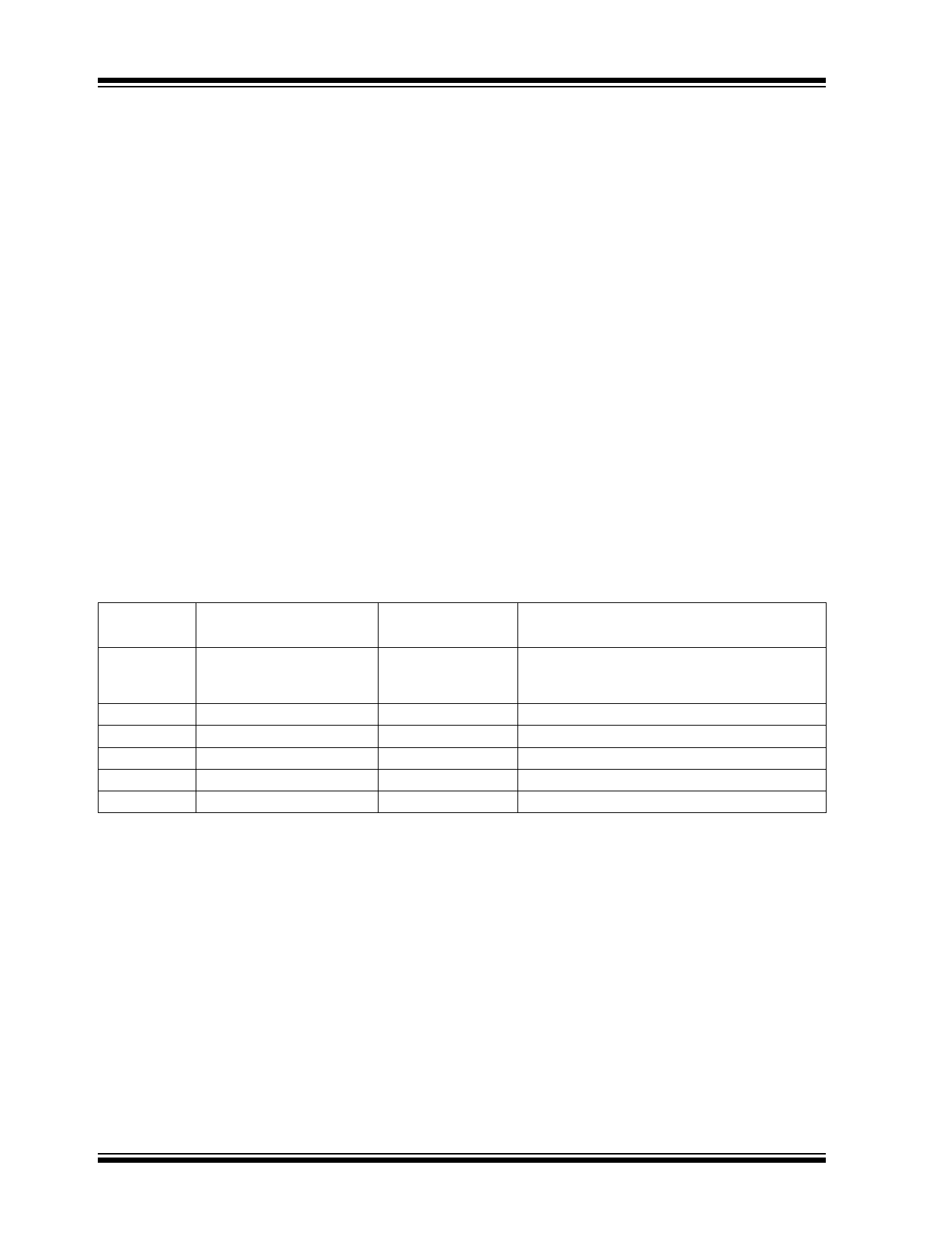
Table 3-2 describes the RMII signals. Refer to RMII Specification v1.2 for detailed information.
TABLE 3-2: RMII SIGNAL DEFINITION
RMII Signal
Name
REF_CLK
TXEN
TXD[1:0]
CRS_DV
RXD[1:0]
RXER
Direction with Respect to
PHY KSZ8051RNL Signal
Output (25 MHz clock
mode)/<no connect>
(50 MHz clock mode)
Input
Input
Output
Output
Output
Direction with
Respect to MAC
Description
Input/Input or
<no connect>
Synchronous 50 MHz reference clock for
receive, transmit, and control interface
Output
Transmit Enable
Output
Transmit Data[1:0]
Input
Carrier Sense/Receive Data Valid
Input
Receive Data[1:0]
Input or not required Receive Error
3.3.4 REFERENCE CLOCK (REF_CLK)
REF_CLK is a continuous 50 MHz clock that provides the timing reference for TXEN, TXD[1:0], CRS_DV, RXD[1:0] and
RX_ER.
For 25 MHz clock mode, the KSZ8051RNL generates and outputs the 50 MHz RMII REF_CLK to the MAC at REF_CLK
(pin 19).
For 50 MHz clock mode, the KSZ8051RNL takes in the 50 MHz RMII REF_CLK from the MAC or system board at XI
(pin 9) and leaves the REF_CLK (pin 19) as a no connect.
3.3.5 TRANSMIT ENABLE (TXEN)
TXEN indicates that the MAC is presenting dibits on TXD[1:0] for transmission. It is asserted synchronously with the first
dibit of the preamble and remains asserted while all dibits to be transmitted are presented on the RMII. It is negated
before the first REF_CLK following the final dibit of a frame.
TXEN transitions synchronously with respect to REF_CLK.
DS00002310A-page 20
2016 Microchip Technology Inc.
Share Link: 