AD607 Просмотр технического описания (PDF) - Analog Devices
Номер в каталоге
Компоненты Описание
производитель
AD607 Datasheet PDF : 24 Pages
| |||
AD607
VPOS
AD607
RT
2RT
IFOP
BPF
2RT
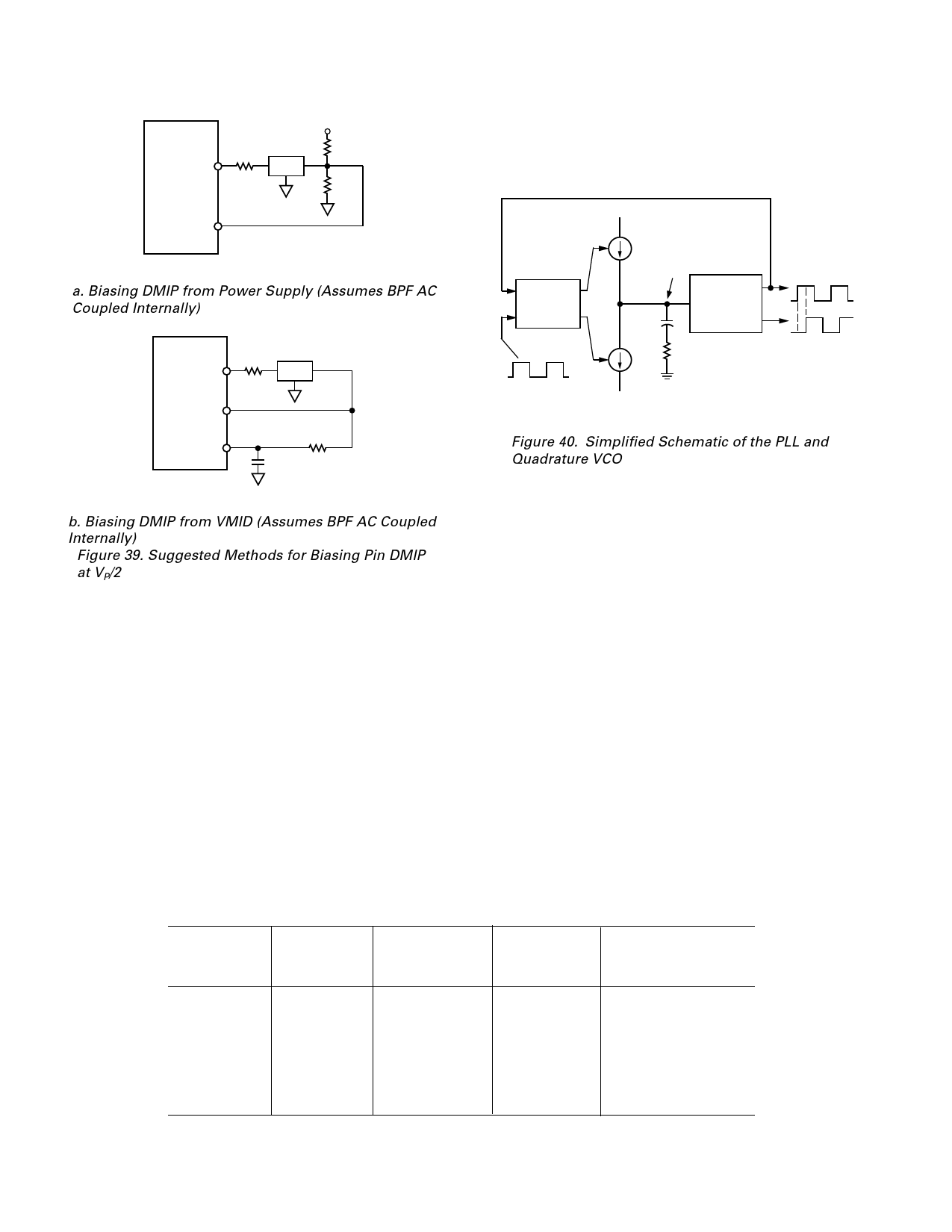
quadrature accuracy of this VFQO is typically –1.2° at
10.7 MHz. The PLL uses a sequential-phase detector that
comprises low power emitter-coupled logic and a charge pump
(Figure 40).
DMIP
a. Biasing DMIP from Power Supply (Assumes BPF AC
Coupled Internally)
AD607
RT
IFOP
BPF
DMIP
DMIP
RT
CBYPASS
b. Biasing DMIP from VMID (Assumes BPF AC Coupled
Internally)
Figure 39. Suggested Methods for Biasing Pin DMIP
at VP/2
For IFs < 3 MHz, the on-chip low-pass filters (2 MHz cutoff)
do not attenuate the IF or feedthrough products; thus, the maxi-
mum input voltage at DMIP must be limited to ± 75 mV to al-
low sufficient headroom at the I and Q outputs for not only the
desired baseband signal but also the unattenuated higher-order
demodulation products. These products can be removed by an
external low-pass filter. In the case of IS54 applications using a
455 kHz IF and the AD7013 baseband converter, a simple
1-pole RC filter with its corner above the modulation bandwidth
is sufficient to attenuate undesired outputs.
Phase-Locked Loop
The demodulators are driven by quadrature signals that are pro-
vided by a variable frequency quadrature oscillator (VFQO),
phase locked to a reference signal applied to pin FDIN. When
this signal is at the IF, inphase and quadrature baseband out-
puts are generated at IOUT and QOUT, respectively. The
F
SEQUENTIAL U
PHASE
R
DETECTOR D
REFERENCE CARRIER
(FDIN AFTER LIMITING)
IU~
40µA
VF
VARIABLE-
FREQUENCY
QUADRATURE
C OSCILLATOR
ID~
R
40µA
I-CLOCK
90°
Q-CLOCK
(ECL OUTPUTS)
Figure 40. Simplified Schematic of the PLL and
Quadrature VCO
The reference signal may be provided from an external source,
in the form of a high-level clock, typically a low level signal
(± 400 mV) since there is an input amplifier between FDIN and
the loop’s phase detector. For example, the IF output itself can
be used by connecting DMIP to FDIN, which will then pro-
vide automatic carrier recover for synchronous AM detection
and take advantage of any post-IF filtering. Pin FDIN must be
biased at VP/2; Figure 41 shows suggested methods.
The VFQO operates from 400 kHz to 12 MHz and is con-
trolled by the voltage between VPOS and FLTR. In normal op-
eration, a series RC network, forming the PLL loop filter, is
connected from FLTR to ground. The use of an integral
sample-hold system ensures that the frequency-control voltage
on pin FLTR remains held during power-down, so reacquisition
of the carrier typically occurs in 16.5 µs.
In practice, the probability of a phase mismatch at power-up is
high, so the worst-case linear settling period to full lock needs
to be considered in making filter choices. This is typically 16.5 µs
at an IF of 10.7 MHz for a ± 100 mV signal at DMIP and
FDIN.
Table II. AD607 Gain and Manual Gain Control Voltage vs. Power Supply Voltage
Power Supply
Voltage
(V)
GREF
(= VMID)
(V)
Scale Factor Scale Factor
(dB/V)
(mV/dB)
Gain Control
Voltage Input Range
(V)
2.7
1.35
55.56
18.00
0.360–1.800
3.0
1.5
50.00
20.00
0.400–2.000
3.5
1.75
42.86
23.33
0.467–2.333
4.0
2.0
37.50
26.67
0.533–2.667
4.5
2.25
33.33
30.00
0.600–3.000
5.0
2.5
30.00
33.33
0.667–3.333
5.5
2.75
27.27
36.67
0.733–3.667
NOTE
Maximum gain occurs for gain control voltage = 0 V.
–16–
REV. 0
Share Link: 