DJLXT908LC Просмотр технического описания (PDF) - Intel
Номер в каталоге
Компоненты Описание
производитель
DJLXT908LC Datasheet PDF : 44 Pages
| |||
LXT908 — Universal 3.3V 10BASE-T and AUI Transceiver
2.1.2
Transmit Function
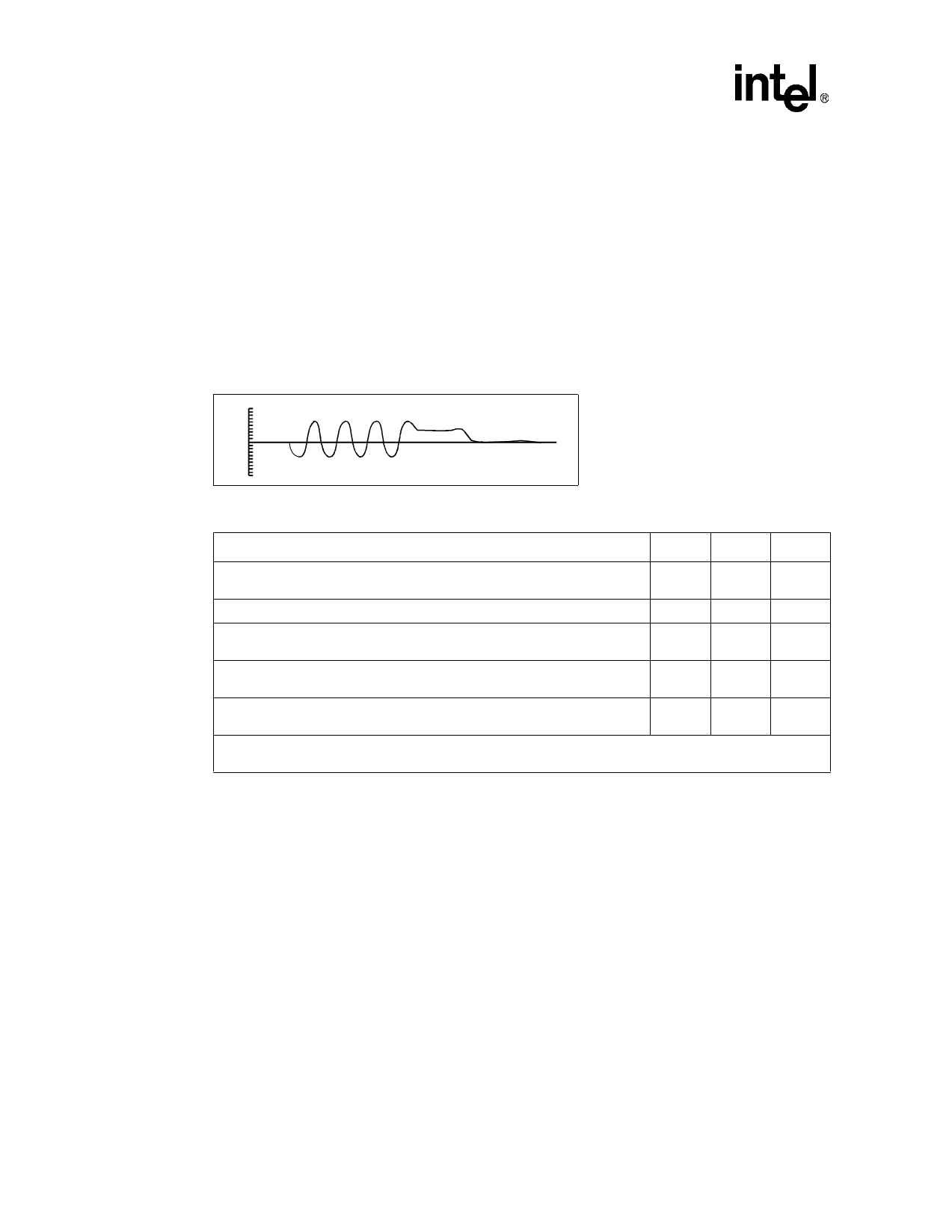
The LXT908 receives NRZ data from the controller at the TXD input as shown in Figure 1,
“LXT908 Block Diagram” on page 7, and passes it through a Manchester encoder. The encoded
data is then transferred to either the AUI cable (the DO circuit) or the twisted-pair network (the
TPO circuit). The advanced integrated pulse shaping and filtering network produces the output
signal on TPON and TPOP, shown in Figure 3. The TPO output is pre-distorted and pre-filtered to
meet the 10BASE-T jitter template. An internal continuous resistor-capacitor filter is used to
remove any high-frequency clocking noise from the pulse shaping circuitry. Integrated filters
simplify the design work required for FCC-compliant EMI performance. During idle periods, the
LXT908 transmits link integrity test pulses on the TPO circuit (if LI is enabled and integrated PLS/
MAU mode is selected). External resistors control the termination impedance.
Figure 3. LXT908 TPO Output Waveform
4V
2V
0V
-2V
-4V
Table 2. Controller Compatibility Mode Options
Controller Mode
MD2
MD1
MD0
Mode 1 - For AMD AM7990, Motorola 68EN360, MPC860 or compatible
controllers
Low
Low
Low
Mode 2 - For Intel 82596 or compatible controllers
Low
Low
High
Mode 3 - For Fujitsu MB86950, MB86960 or compatible controllers (Seeq
8005)1
Low
High
Low
Mode 4 - For National Semiconductor 8390 or compatible controllers (TI
TMS380C26)
Low
High
High
Mode 5 - For custom controllers (Mode 3 with TCLK, RCLK and COL
inverted)
High
High
Low
1. SEEQ controllers require inverters on CLKI, LBK, RCLK, and COL in Mode 3; or on CLKI, LBK, and TCLK
in Mode 5.
2.1.3
Jabber Control Function
Figure 4 on page 13 is a state diagram of the LXT908 Jabber control function. The LXT908 on-
chip Watch-Dog Timer prevents the DTE from locking into a continuous transmit mode. When a
transmission exceeds the time limit, the Watch-Dog Timer disables the transmit and loopback
functions, and activates the JAB pin. Once the LXT908 is in the jabber state, the TXD circuit must
remain idle for a period of 0.25 to 0.75 seconds before it will exit the jabber state.
12
Datasheet
Document #: 249049
Revision #: 002
Rev. Date: June 19, 2001
Share Link: 