CXP82540 Просмотр технического описания (PDF) - Sony Semiconductor
Номер в каталоге
Компоненты Описание
производитель
CXP82540 Datasheet PDF : 20 Pages
| |||
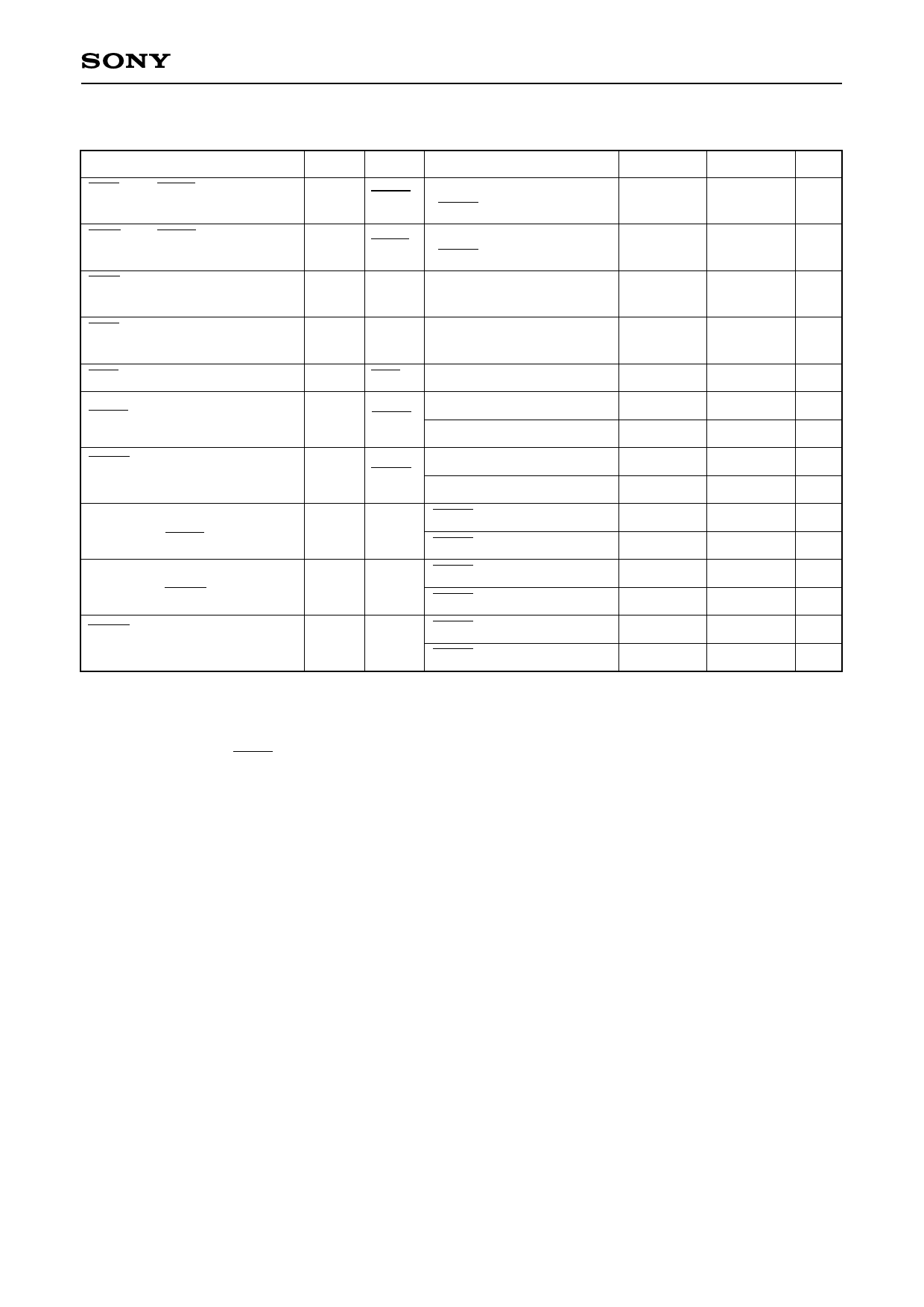
CXP82532/82540
(2) Serial transfer (CH0)
(Ta = –20 to +75°C, VDD = 4.5 to 5.5V, Vss = 0V)
Item
Symbol Pin
Condition
Min.
Max. Unit
CS0 ↓ → SCK0
delay time
CS0 ↑ → SCK0
float delay time
CS0 ↓ → SO0
delay time
tDCSK SCK0
tDCSKF SCK0
Chip select transfer mode
(SCK0 = output mode)
Chip select transfer mode
(SCK0 = output mode)
tDCSO SO0 Chip select transfer mode
tsys + 200 ns
tsys + 200 ns
tsys + 200 ns
CS0 ↑ → SO0
float delay time
CS0 high level width
SCK0 cycle time
SCK0
high and low level width
SI0 input setup time
(against SCK0 ↑)
SI0 input hold time
(against SCK0 ↑)
SCK0 ↓ → SO0
delay time
tDCSOF SO0 Chip select transfer mode
tsys + 200 ns
tWHCS CS0 Chip select transfer mode tsys + 200
ns
Input mode
2tsys + 200
ns
tKCY SCK0
Output mode
16000/fc
ns
tKH
tKL
Input mode
SCK0
Output mode
tsys + 100
8000/fc – 50
ns
ns
SCK0 input mode
100
ns
tSIK SI0
SCK0 output mode
200
ns
SCK0 input mode
tsys + 200
ns
tKSI SI0
SCK0 output mode
100
ns
tKSO SO0
SCK0 input mode
SCK0 output mode
tsys + 200 ns
100
ns
Note 1) tsys is determind by the upper two bits of the clock control resister (Address: 00FEH; CPU clock
selected) resulting in one of the 3 following values:
tsys [ns] = 2000/fc (Upper 2 bits = "00"), 4000/fc (Upper 2 bits = "01"), 16000/fc (Upper 2 bits = "11")
Note 2) The load of SCK0 output mode and SO0 output delay time is 50pF + 1TTL.
– 14 –
Share Link: 