UC3842BN Просмотр технического описания (PDF) - Motorola => Freescale
Номер в каталоге
Компоненты Описание
производитель
UC3842BN Datasheet PDF : 16 Pages
| |||
UC3842B, 43B UC2842B, 43B
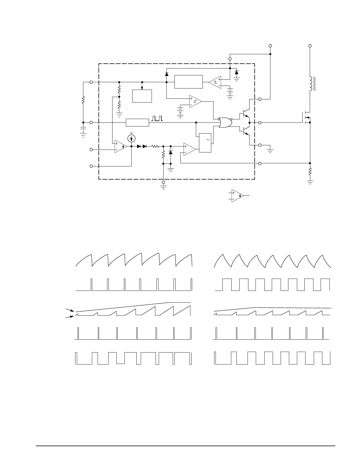
Figure 17. Representative Block Diagram
VCC
Vin
VCC 7(12)
Vref
8(14)
RT
2.5V
R Internal
Bias
R
CT 4(7)
Voltage
Feedback
Input 2(3)
Output/
Compensation 1(1)
Oscillator
+ 1.0mA
2R
Error
R
Amplifier
Reference
Regulator
VCC
UVLO
+
–
3.6V
+
–
Vref
UVLO
S
Q
R
PWM
Latch
1.0V
Current Sense
Comparator
Gnd 5(9)
Pin numbers adjacent to terminals are for the 8–pin dual–in–line package.
Pin numbers in parenthesis are for the D suffix SO–14 package.
36V
(See
Text)
VC
7(11)
Output
Q1
6(10)
Power Ground
5(8)
Current Sense Input
3(5)
RS
= Sink Only Positive True Logic
Capacitor CT
Latch
“Set” Input
Output/
Compensation
Current Sense
Input
Latch
“Reset” Input
Output
Figure 18. Timing Diagram
Large RT/Small CT
Small RT/Large CT
MOTOROLA ANALOG IC DEVICE DATA
9
Share Link: 