LC05111C13MTTTG Просмотр технического описания (PDF) - ON Semiconductor
Номер в каталоге
Компоненты Описание
производитель
LC05111C13MTTTG
ON Semiconductor

LC05111C13MTTTG Datasheet PDF : 17 Pages
| |||
LC05111CMT
Specifications
Table 1. ABSOLUTE MAXIMUM RATINGS TA = 25°C (Notes 1 and 2)
Parameter
Symbol
Ratings
Unit
Conditions
Supply voltage
VCC
−0.3 to +12.0
V
Between PAC+ and VCC : R1 = 680 W
S1 − S2 voltage
VS1−S2
24.0
V
CS terminal Input voltage
CS
VCC−24.0
V
Charge or discharge current
BAT−, PAC−
10.0
A
TST Input voltage
TST
−0.3 to +7.0
V
Storage temperature
Tstg
−55 to +125
°C
Current between S1 and S2(DC)
ID
10.0
A
VCC = 3.7 V
Current between S1 and S2
IDP
(continuous pulse)
35
A
Pulse Width < 10 ms, duty cycle < 1%
Operating ambient temperature
Topr
−40 to +85
°C
Allowable power dissipation
Pd
450
mW
Glass epoxy four−layer board. Board
size 27.4 mm x 3.1 mm x 0.8 mm
Junction temperature
Tj
125
°C
Stresses exceeding those listed in the Maximum Ratings table may damage the device. If any of these limits are exceeded, device functionality
should not be assumed, damage may occur and reliability may be affected.
1. Absolute maximum ratings represent the values which cannot be exceeded at any given time.
2. If you intend to use this IC continuously under high temperature, high current, high voltage, or drastic temperature change, even if it used
within the range of absolute maximum ratings or operating conditions, there is a possibility of decrease reliability. Please contact us for
confirmation.
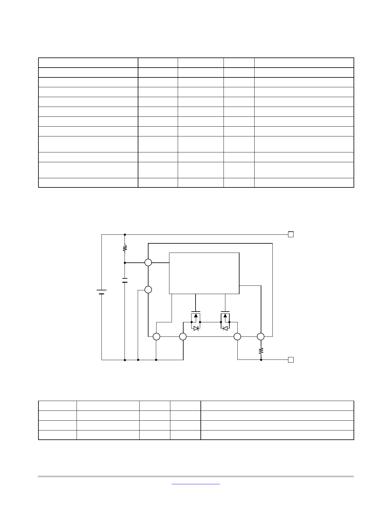
PAC+
R1
VCC
Battery
C1
TST
Controller IC
VSS
S1
S2
CS
R2
Figure 1. Example of Application Circuit
PAC−
Table 2.
Components Recommended Value
Max
Unit
Description
R1
680
1k
W
R2
1k
2k
W
C1
0.1 m
1.0 m
F
3. We don’t guarantee the characteristics of the circuit shown above.
4. TST pin would be better to be connected to VSS pin, though it is connected to VSS with internal resistor (100 kW typ).
5. Battery voltage drop occurs, a current of about 60 mA flow period of 1.5 V − 1.3 V.
www.onsemi.com
2
Share Link: