V363EPC Просмотр технического описания (PDF) - QuickLogic Corporation
Номер в каталоге
Компоненты Описание
производитель
V363EPC Datasheet PDF : 23 Pages
| |||
DC Specifications
PCI Bus DC Specifications
4.1
PCI Bus DC Specifications
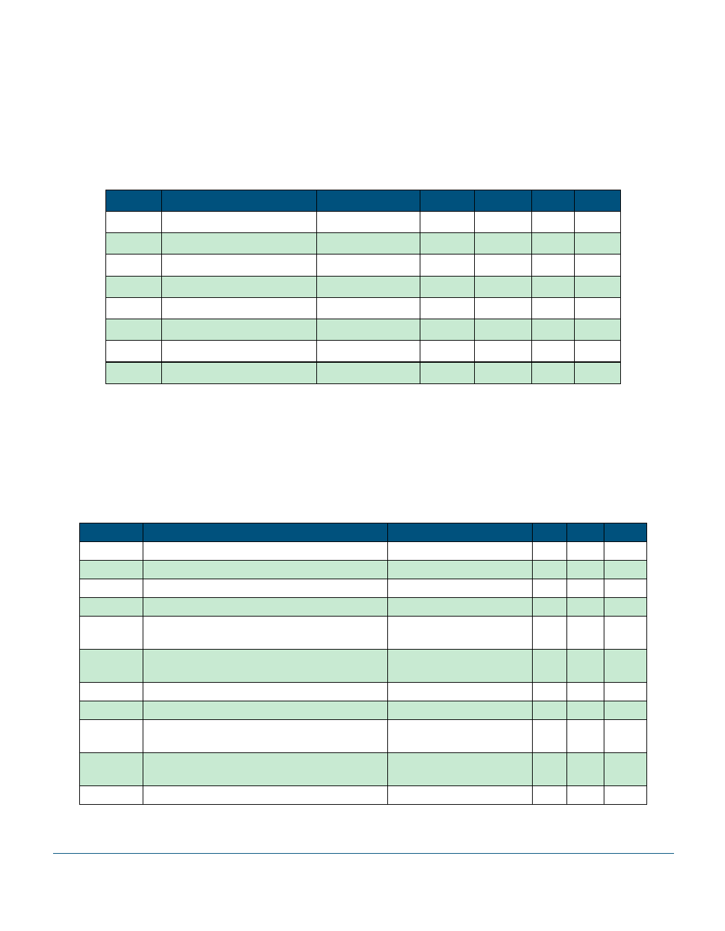
Table 12: PCI Bus Signals DC Operating Specifications
Symbol
Parameter
Condition
Min
Max Units
VIH
VIL
IIL
VOH
VOL
CIN
CCLK
CIDSEL
Input high voltage
Input low voltage
Input leakage current
Output high voltage
Output low voltage
Input pin capacitance
PCLK pin capacitance
IDSEL pin capacitance
0.5 VCC 5.75
V
−0.5 0.3 VCC V
0 < VIN < VCC
±10
µA
IOUT = −500 µA 0.9 VCC
V
IOUT = 1500 µA
0.1 VCC V
10
pF
5
12
pF
8
pF
1. Custom 5 V tolerant PCI buffers are used in the design.
2. Input leakage currents include hi-Z output leakage for all bi-directional buffers with tri-state outputs.
3. Absolute maximum pin capacitance for a PCI unit is 10 pF (except for CLK).
4. Lower capacitance on this input-only pin allows for non-resistive coupling to AD[xx].
Notes
1
2
3
4
4.2 Local Bus DC Specifications
Table 13: Local Bus Signals DC Operating Specifications
Symbol
VIL
VIH
IIL
IIH
VOL4
VOH4
IOZL
IOZH
ICC (max)
ICC (typ)
CIO
Description
Low level input voltage
High level input voltage
Low level input current
High level input current
Low level output voltage for 4 mA
outputs and I/O pins
High level output voltage for 4 mA
outputs and I/O pins
Low level float input leakage
High level float input leakage
Maximum supply current
Typical supply current
Input and output capacitance
Conditions
VIN = GND
VIN = VCC
IOL = 4 mA
Min Max Units
0.8 V
2.0
V
−10
µA
10 µA
0.4 V
IOH = −4 mA
2.4
V
VIN = GND
−10
µA
VIN = VCC
10 µA
VCC = 3.6 V
PCLK = LCLK = 33 MHz
55 mA
VCC = 3.3 V
PCLK = LCLK = 33 MHz
44 mA
10 pF
18
V363EPC A0 Data Sheet Rev 1.01 DS-EC301-0101
© 2000 V3 Semiconductor Corp.
Share Link: 