EN80960SA16512 Просмотр технического описания (PDF) - Intel
Номер в каталоге
Компоненты Описание
производитель
EN80960SA16512 Datasheet PDF : 39 Pages
| |||
80960SA
2.0 ELECTRICAL SPECIFICATIONS
2.1 Power and Grounding
The 80960SA is implemented in CHMOS IV
technology and therefore has modest power require-
ments. Its high clock frequency and numerous output
buffers (address/data, control, error and arbitration
signals) can cause power surges as multiple output
buffers simultaneously drive new signal levels. For
clean on-chip power distribution, VCC and VSS pins
separately feed the device’s functional units. Power
and ground connections must be made to all
80960SA power and ground pins. On the circuit
board, all VCC pins must be strapped closely
together, preferably on a power plane; all VSS pins
should be strapped together, preferably on a ground
plane.
2.2 Power Decoupling
Recommendations
Place a liberal amount of decoupling capacitance
near the 80960SA. When driving the bus the
processor can cause transient power surges, partic-
ularly when connected to a large capacitive load.
Low inductance capacitors and interconnects are
recommended for best high frequency electrical
performance. Inductance is reduced by shortening
board traces between the processor and decoupling
capacitors as much as possible.
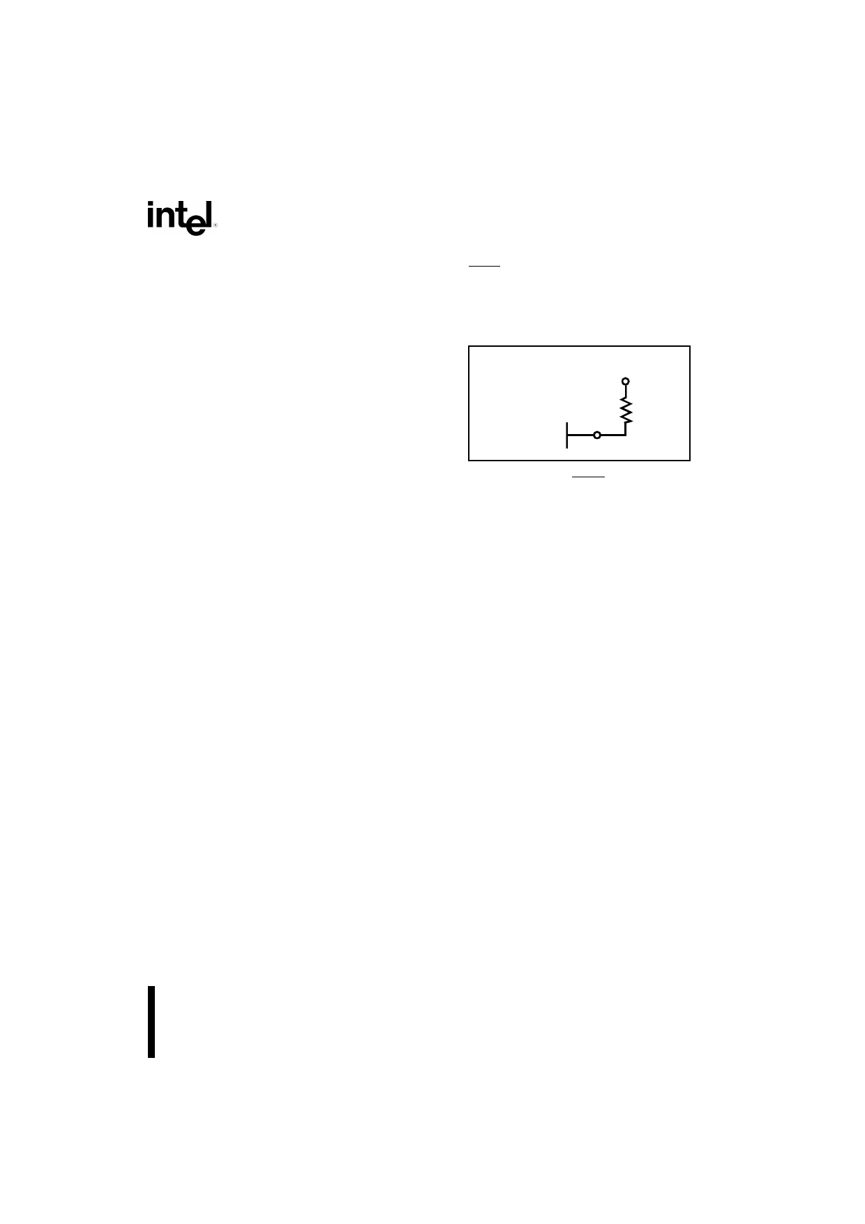
The LOCK open-drain pin requires a pullup resistor
whether or not the pin is used as an output. Figure 5
shows the recommended resistor value.
Do not connect external logic to pins marked NC.
OPEN-DRAIN
OUTPUT
VCC
910Ω
Figure 5. Connection Recommendation
for LOCK
2.4 Characteristic Curves
Figure 6 shows typical supply current requirements
over the operating temperature range of the
processor at supply voltage (VCC) of 5V. Figure 7
shows the typical power supply current (ICC) that the
80960SA requires at various operating frequencies
when measured at three input voltage (VCC) levels.
For a given output current (IOL) the curve in Figure 8
shows the worst case output low voltage (VOL).
Figure 9 shows the typical capacitive derating curve
for the 80960SA measured from 1.5V on the system
clock (CLK) to 0.8V on the falling edge and 2.0V on
the rising edge of the bus address/data (AD) signals.
2.3 Connection Recommendations
For reliable operation, always connect unused inputs
to an appropriate signal level. In particular, if one or
more interrupt lines are not used, they should be
pulled up. No inputs should ever be left floating.
11
Share Link: 