LC5824 Просмотр технического описания (PDF) - SANYO -> Panasonic
Номер в каталоге
Компоненты Описание
производитель
LC5824 Datasheet PDF : 24 Pages
| |||
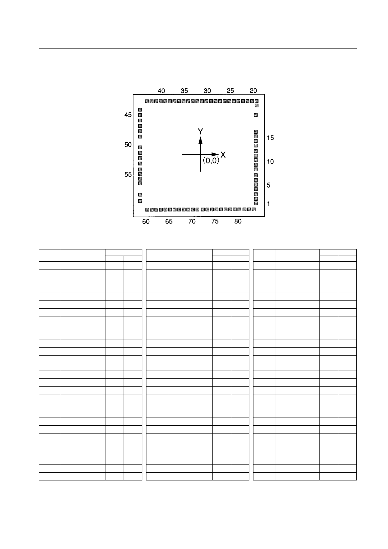
Pad Arrangement
Chip size: 4.92 mm × 5.15 mm
Pad size: 120 µm × 120 µm
Chip thickness 480 µm (chip specifications)
LC5824, LC5823, LC5822
Pad Coordinates
PAD No.
Pin
60 Seg 22
61 Seg 23
62 Seg 24
63 Seg 25
64 Seg 26
65 Seg 27
66 Seg 28
67 Seg 29
68 Seg 30
69 Seg 31
70 Seg 32
71 Seg 33
72 Seg 34
73 Seg 35
74 Seg 36
75 Seg 37
76 Seg 38
77 Seg 39
78 Seg 40
79 Seg 41
80 Seg 42
81 XC
82 XTOUT
83 XTIN
1
VDD
2
VSS
3 CFIN/P1
4 CFOUT/P2
Coordinates
X µm Y µm
–2030 –2178
–1850 –2178
–1670 –2178
–1490 –2178
–1310 –2178
–1130 –2178
–950 –2178
–770 –2178
–590 –2178
–410 –2178
–230 –2178
–50 –2178
122 –2178
302 –2178
482 –2178
662 –2178
842 –2178
1022 –2178
1202 –2178
1382 –2178
1562 –2178
1774 –2178
1954 –2178
2134 –2178
2257 –1959
2257 –1779
2257 –1599
2257 –1402
PAD No.
Pin
5
VDD3
6
VDD2/BAK
7
VDD1
8 ALM
9 SO1
10 SO2 I/O port
11 SO3 I/O port
12 SO4 I/O port
13 M1
14 M2 I/O port
15 M3 I/O port
16 M4 I/O port
17 RES I/O port
18 Test
19 Test
20 TST
21 CUP1
22 CUP2
23 Seg 1
24 Seg 2
25 Seg 3
26 Seg 4
27 Seg 5
28 Seg 6
29 Seg 7
30 Seg 8
31 Seg 9
32 Seg 10
Coordinates
X µm Y µm
2257 –1212
2257 –1032
2257 –852
2257 –601
2257 –419
2257 –236
2257
56
2257 132
2257 364
2257 544
2257 724
2257 904
2257 1636
2330 1998
2330 2178
2150 2178
1970 2178
1790 2178
1606 2178
1426 2178
1246 2178
1066 2178
886 2178
706 2178
526 2178
346 2178
166 2178
–14 2178
PAD No.
Pin
33 Seg 11
34 Seg 12
35 Seg 13
36 Seg 14
37 Seg 15
38 Seg 16
39 Seg 17
40 Seg 18
41 Seg 19
42 Seg 20
43 Seg 21
44 COM1
45 COM2
46 S1
47 S2 Input port
48 S3 Input port
49 S4 Input port
50 K1
51 K2 Input port
52 K3 Input port
53 K4 Input port
54 A1
55 A2 I/O ports
56 A3 I/O ports
57 A4 I/O ports
58 COM3/P3
59 COM4/P4
Note: • The pin numbers are the QIP-80E mass-production package pin numbers.
• The test pin (TST) must be connected to VSS.
• Pads number 42 and 43 in the chip version must be left open.
• Do not use solder dip techniques to mount the QIP-80E package version.
• In the chip version, the substrate must be either connected to VSS or left open.
Coordinates
X µm Y µm
–194 2178
–374 2178
–546 2178
–726 2178
–906 2178
–1086 2178
–1266 2178
–1446 2178
–1626 2178
–1806 2178
–1986 2178
–2270 1871
–2270 1628
–2270 1367
–2270 1140
–2270 960
–2270 734
–2270 328
–2270
88
–2270 –140
–2270 –380
–2270 –593
–2270 –773
–2270 –953
–2270 –1133
–2270 –1602
–2270 –1846
No. 5944-4/24
Share Link: 