LA1193M Просмотр технического описания (PDF) - SANYO -> Panasonic
Номер в каталоге
Компоненты Описание
производитель
LA1193M Datasheet PDF : 22 Pages
| |||
LA1193M, 1193V
• Wide AGC circuit
The wide AGC sensitivity is set by the value of the capacitor on pin 8. However, since incorrect operation due to the
local oscillator signal may occur if this capacitor is too large, its value must be chosen carefully.
• 3D-AGC
If the difference in sensitivity between the N-AGC and the W-AGC systems is too large during 3D-AGC operation,
the S/N ratio can be degraded in the vicinity of the input where the AGC switches. Therefore, the 3D-AGC setting
values must be selected carefully. Although this problem can be ameliorated by applying a time constant to pin 20, in
principle, this S/N ratio degradation should be prevented by limiting the sensitivity difference between the two AGC
systems.
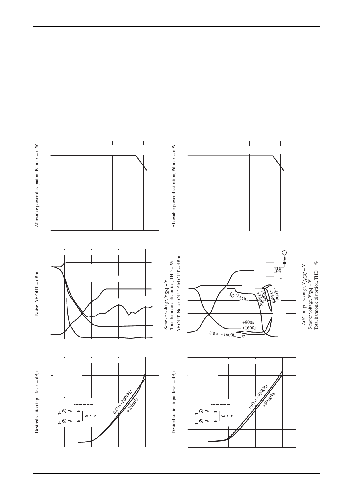
Pd max -- Ta
[LA1193V]
600
When mounted on a 23×36×1.6mm3 glass epoxy
printed circuit board
500
400
300
200
100
0-40
-20
0
20
40
60
Ambient temperature, Ta -- °C
I/O characteristics
0
3SK251+LA1193M or 1193V+LA1145M
S+N
-20
VCC = 8.0V, fr = 83MHz
fm = 1kHz, dev22.5kHz
Audio Filter, IHF-BPF T/200
-40
VSM
80 85 100
JK119329
8
6
-60
AM OUT
30%mod
fm = 1kHz
4
-80
N
2
THD
-100-20
0
0
20
40
60
80 100 120 140
Antenna input level -- dBµ
JK119331
Two-signal interference characteristics
50
3SK251+LA1193M or 1193V+LA1145M
VCC = 8.0V
fr = 83MHz
40 fm = 1kHz
dev = 22.5kHz
fuD = fr ± ∆f
30 non dev
Dummy two - signal input
75Ω 24Ω
20
24Ω
75Ω 24Ω
ANT
input
10
0
50
60
70
80
90 100 110 120 130
Interfering station input level -- dBµ JK119333
Pd max -- Ta
[LA1193M]
600
When mounted on a 41×30×1.1mm3 glass epoxy
printed circuit board
500
400
300
200
100
0-40
-20
0
20
40
60
Ambient temperature, Ta -- °C
I/O characteristics
40
VCC = 8.0V
20
fD = fr = 83MHz
fm = 1kHz
dev = 22.5kHz
fD VSM
Mix
0
80 85 100
JK119330
14
13
510Ω
51pF 12
10
fD S+N
-20
fuD S+N
8
-40
fD VAGC
6
-60
-80
-100
-20
fuD N
4
fD N
+800k,
+1600k
fuD VSM
2
−800k, −1600k
fuD VAGC
0
0
20 40 60 80 100 120 140 160
Antenna input level -- dBµ
JK19332
Two-signal interference characteristics
50
3SK251+LA1193M or 1193V+LA1145M
VCC = 8.0V
fr = 83MHz
40 fm = 1kHz
dev = 22.5kHz
fuD = fr ± ∆f
30 non dev
Dummy two - signal input
75Ω 24Ω
20
75Ω
75Ω 24Ω
ANT
input
10
0
50
60
70
80
90 100 110 120 130
Interfering station input level -- dBµ JK119334
No.4715-13/22
Share Link: 