RF2174PCBA-41X Просмотр технического описания (PDF) - RF Micro Devices
Номер в каталоге
Компоненты Описание
производитель
RF2174PCBA-41X Datasheet PDF : 16 Pages
| |||
RF2174
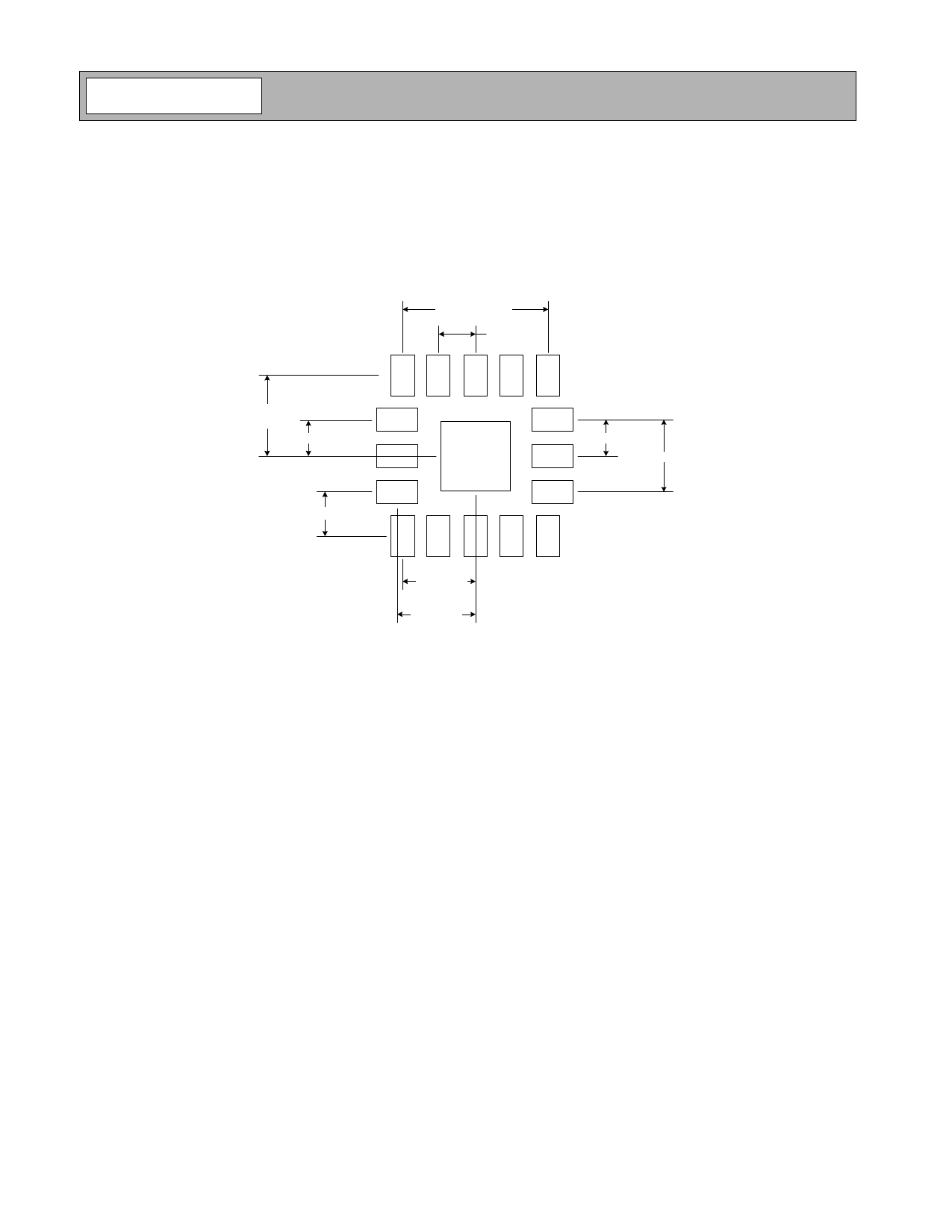
PCB Solder Mask Pattern
Liquid Photo-Imageable (LPI) solder mask is recommended. The solder mask footprint will match what is shown for the
PCB Metal Land Pattern with a 3mil expansion to accommodate solder mask registration clearance around all pads. The
center-grounding pad shall also have a solder mask clearance. Expansion of the pads to create solder mask clearance
can be provided in the master data or requested from the PCB fabrication supplier.
A = 0.71 x 1.09 (mm) Typ.
B = 1.09 x 0.71 (mm) Typ.
C = 1.73 (mm) Sq.
3.20 (mm) Typ.
0.81 (mm)
Typ.
Pin 1
A
A
A
A
A
1.73 (mm)
Typ.
B
B
0.81 (mm) Typ.
0.81 (mm) Typ.
B
C
B
1.60 (mm)
B
B
0.94 (mm) Typ.
A
A
A
A
A
1.60 (mm)
Typ.
1.73 (mm)
Typ.
Figure 2. PCB Solder Mask Pattern (Top View)
Thermal Pad and Via Design
The PCB land pattern has been designed with a thermal pad that matches the exposed die paddle size on the bottom of
the device.
Thermal vias are required in the PCB layout to effectively conduct heat away from the package. The via pattern shown
has been designed to address thermal, power dissipation and electrical requirements of the device as well as accommo-
dating routing strategies.
The via pattern used for the RFMD qualification is based on thru-hole vias with 0.203mm to 0.330mm finished hole size
on a 0.5mm to 1.2mm grid pattern with 0.025mm plating on via walls. If micro vias are used in a design, it is suggested
that the quantity of vias be increased by a 4:1 ratio to achieve similar results.
Figure 3. shows the via pattern used for the RFMD qualification design.
2-288
Rev A8 060918
Share Link: 