ADDC02808PBTV/QMLH Просмотр технического описания (PDF) - Analog Devices
Номер в каталоге
Компоненты Описание
производитель
ADDC02808PBTV/QMLH Datasheet PDF : 20 Pages
| |||
ADDC02808PB
Even when the load current steps down to 0.1 A, the maximum
deviation of the output voltage is only about 400 mV, or 5%.
However, it is important to realize that if the next power pulse
occurs before this transient is over, then the output voltage will
not have the response depicted in the last section. This is be-
cause the feedback integrator will not have had time to return
to its normal state, and so the converter’s ability to respond to a
positive step change in load current will be reduced. The maxi-
mum negative going deviation in the output voltage under this
circumstance will then be greater than is shown in the figures of
that section.
Should this situation arise, one approach would be to step the
load current down to an intermediate value (e.g., 4 A) at the
end of the power pulse, and then let this current decay to a
smaller value (e.g., 0.1 A) with a time constant in the 100 µs to
200 µs range. This should permit a rapid return to a steady state
condition at the end of the power pulse without requiring a large
average load current during the low power portion of the cycle.
PIN CONNECTIONS
Pins 1 and 2 (؎SENSE)
Pins 1 and 2 must always be connected for proper operation,
although failure to make these connections will not be cata-
strophic to the converter under normal operating conditions.
Pin 1 must always be connected to the output return and Pin 2
must always be connected to +VOUT. These connections can
be made at any one of the output pins of the converter, or
remotely at the load. A remote connection at the load can
adjust for voltage drops of as much as 0.25 V dc between the
converter and the load.
Long remote sense leads can affect converter stability, although
this condition is rare. The impedance of the long power leads
between the converter and the remote sense point could affect
the converter’s unity gain crossover frequency and phase margin.
Consult factory if long remote sense leads are to be used.
Pin 3 (ADJUST)
An adjustment pin is provided so that the user can change the
nominal output voltage during the prototype stage. Since very
low temperature coefficient resistors are used to set the output
voltage and maintain tight regulation over temperature, using
standard external resistors to adjust the output voltage will
loosen output regulation over temperature. Furthermore, since
the status trip point is not changed when the output voltage is
adjusted using external resistors, the status line will no longer
trip at the standard levels of the newly adjusted output voltage.
If necessary, modified standard units can be ordered with the
necessary changes made inside the package at the factory. The
ADJUST function is sensitive to noise, and care should be
taken in the routing of connections.
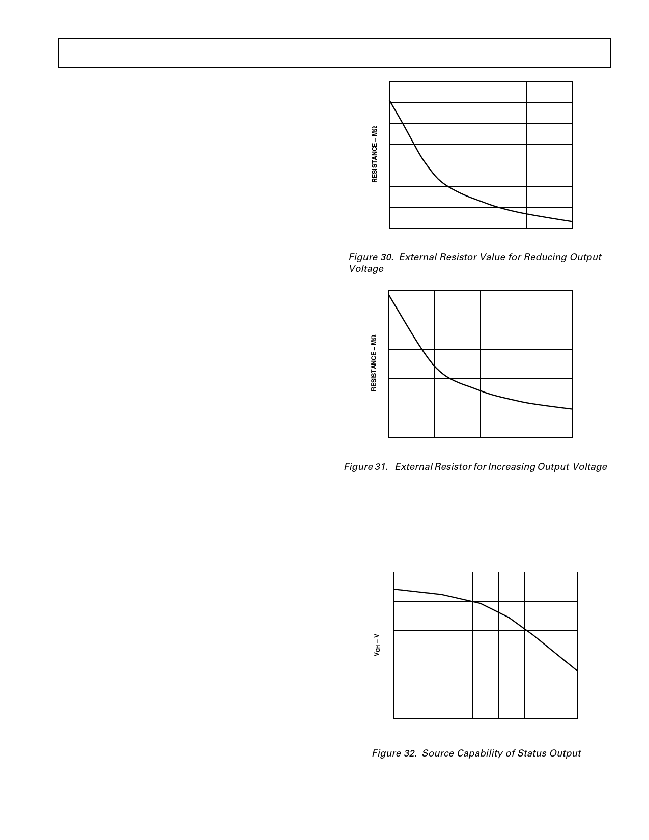
To make the output voltage higher, place a resistor from AD-
JUST (Pin 3) to –SENSE (Pin 1). To make the output voltage
lower, place a resistor from ADJUST (Pin 3) to +SENSE (Pin
2). Figures 30 and 31 show resistor values for a ± 5% change in
output voltage.
With regard to the range that the output voltage can be adjusted
by the user, there are two concerns. As the output voltage is
raised it may become difficult to maintain regulation at full
power and low input voltage. As the output voltage is lowered,
it may become difficult to maintain regulation at minimum
power and high input line.
8
7
6
5
4
3
2
1
99
98
97
96
95
OUTPUT VOLTAGE – %
Figure 30. External Resistor Value for Reducing Output
Voltage
5
4
3
2
1
0
101
102
103
104
105
OUTPUT VOLTAGE – %
Figure 31. External Resistor for Increasing Output Voltage
Pin 4 (STATUS)
Pin 4 is active high referenced to –SENSE (Pin 1), indicating
that the output voltage is typically within ± 5%. The pin is both
pulled up and down by internal circuitry. Figures 32 and 33
show the typical source and sink capabilities of the status out-
put. Refer to the paragraphs describing Pin 3 (ADJUST) for
effect on status trip point.
5
4
3
2
1
0
0.2
0.4
0.6
0.8
1.0
1.2
1.4
1.6
IOH – mA
Figure 32. Source Capability of Status Output
REV. A
–11–
Share Link: 