BTS707 Просмотр технического описания (PDF) - Siemens AG
Номер в каталоге
Компоненты Описание
производитель
BTS707 Datasheet PDF : 12 Pages
| |||
BTS 707
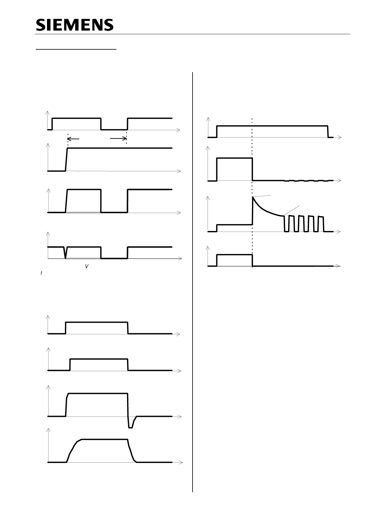
Timing diagrams
Both channels are symmetric and consequently the diagrams are valid for channel 1 and
channel 2
Figure 1a: Vbb turn on, :
Figure 3a: Short circuit:
shut down by overtempertature, reset by cooling
IN
IN
Vbb
td(bb IN)
V
OUT
A
V OUT
normal
operation Output short to GND
I
L
I L(SCp)
I L(SCr)
ST open drain
t
A
in case of too early VIN=high the device may not turn on (curve A)
td(bb IN) approx. 150 µs
Figure 2a: Switching an inductive load
ST
t
Heating up requires several milliseconds, depending on external
conditions. External shutdown in response to status fault signal
recommended.
IN
ST
V
OUT
I
L
t
Semiconductor Group
9
Share Link: 