ATT3042 Просмотр технического описания (PDF) - Unspecified
Номер в каталоге
Компоненты Описание
производитель
ATT3042 Datasheet PDF : 80 Pages
| |||
ATT3000 Series Field-Programmable Gate Arrays
Data Sheet
February 1997
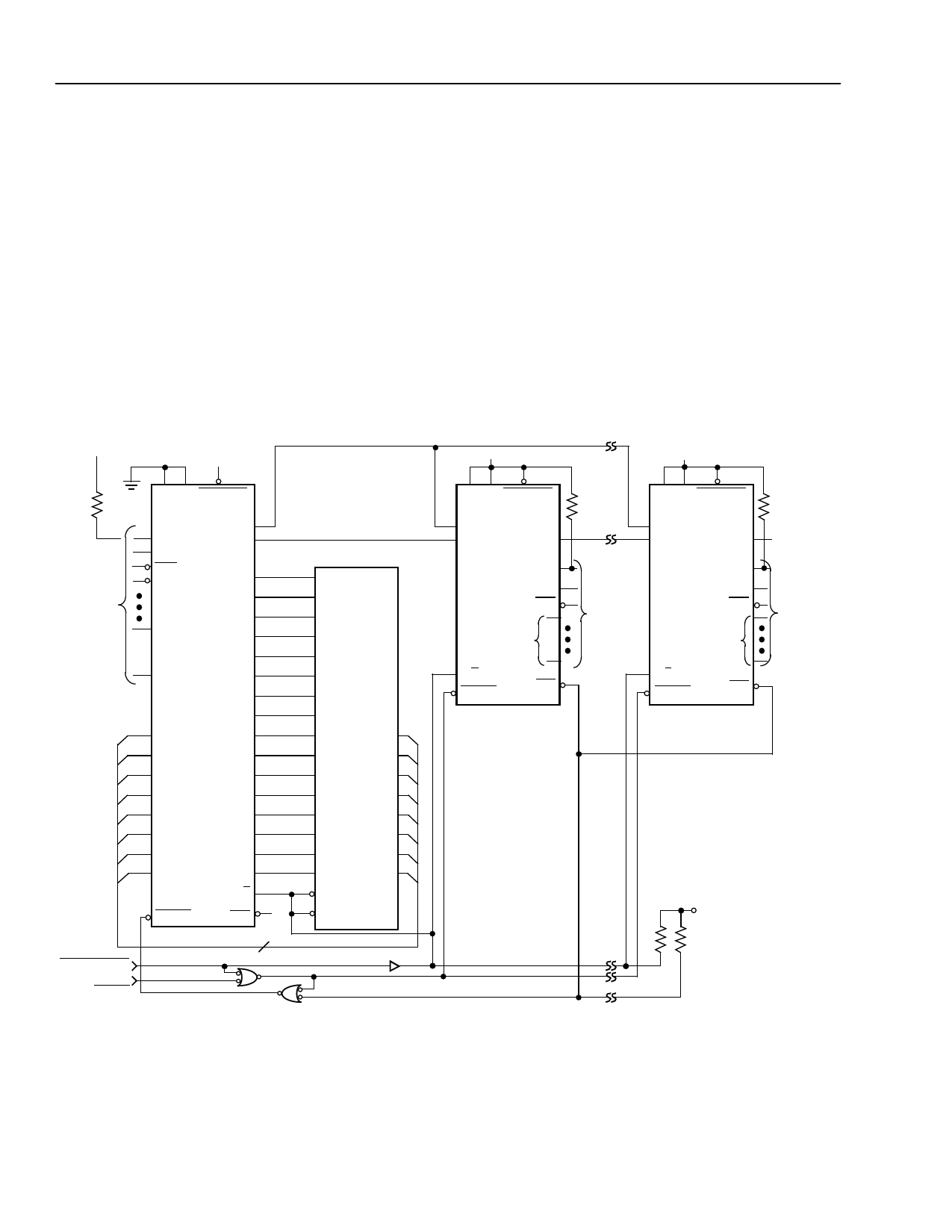
Configuration Modes (continued)
Daisy Chain
The ORCA Foundry for ATT3000 Development System
is used to create a composite configuration bit stream
for selected FPGAs including a preamble, a length
count for the total bit stream, multiple concatenated
data programs, a postamble, plus an additional fill bit
per device in the serial chain. After loading and passing
on the preamble and length count to a possible daisy
chain, a lead device will load its configuration data
frames while providing a high DOUT to possible down-
stream devices as shown in Figure 25. Loading contin-
ues while the lead device has received its configuration
program and the current length count has not reached
the full value. Additional data is passed through the
lead device and appears on the data out (DOUT) pin in
serial form. The lead device also generates the CCLK
to synchronize the serial output data and data in of
downstream FPGAs. Data is read in on DIN of slave
devices by the positive edge of CCLK and shifted out
the DOUT on the negative edge of CCLK. A parallel
master mode device uses its internal timing generator
to produce an internal CCLK of eight times its EPROM
address rate, while a peripheral mode device produces
a burst of eight CCLKs for each chip select and write-
strobe cycle. The internal timing generator continues to
operate for general timing and synchronization of
inputs in all modes.
+5 V
+5 V
+5 V
+5 V
5 kΩ
GENERAL-
PURPOSE
USER I/O
PINS
REPROGRAM
SYSTEM
RESET
M0 M1 PWRDWN
M2
HDC
LDC
RCLK
CCLK
DOUT
A15
A14
A13
A12
OTHER
I/O PINS
A11
A10
FPGA A9
MASTER A8
D7
A7
D6
A6
D5
A5
D4
A4
D3
A3
D2
A2
D1
A1
D0
A0
D/P
RESET
INIT
8
A15
A14
A13 EPROM
A12
A11
A10
A9
A8
A7
D7
A6
D6
A5
D5
A4
D4
A3
D3
A2
D2
A1
D1
A0
D0
OE
CE
OPEN COLLECTOR
M0 M1 PWRDWN
CCLK
DIN
DOUT
FPGA
M2
SLAVE #1 HDC
LDC
OTHER
I/O PINS
D/P
RESET
INIT
5 kΩ
M0 M1 PWRDWN
CCLK
DIN
DOUT
GENERAL-
PURPOSE
USER I/O
FPGA M2
SLAVE #n HDC
LDC
OTHER
I/O PINS
D/P
RESET
INIT
5 kΩ
GENERAL-
PURPOSE
USER I/O
+5 V
5 kΩ EACH
5-3116(F)
Figure 25. Master Mode with Daisy-Chained Slave Mode Devices
26
Lucent Technologies Inc.
Share Link: 