AD61009ARSZ Просмотр технического описания (PDF) - Analog Devices
Номер в каталоге
Компоненты Описание
производитель
AD61009ARSZ Datasheet PDF : 24 Pages
| |||
AD61009
USING THE AD61009
In this section, we will focus on a few areas of special impor-
tance and include a few general application tips. As is true of
any wideband high gain component, great care is needed in PC
board layout. The location of the particular grounding points
must be considered with due regard to possibility of unwanted
signal coupling, particularly from IFOP to RFHI or IFHI or both.
The high sensitivity of the AD61009 leads to the possibility that
unwanted local EM signals may have an effect on the performance.
During system development, carefully-shielded test assemblies
should be used. The best solution is to use a fully-enclosed
box enclosing all components, with the minimum number of
needed signal connectors (RF, LO, I and Q outputs) in min-
iature coax form.
The I and Q output leads can include small series resistors
(about 100 Ω) inside the shielded box without significant loss
of performance, provided the external loading during testing
is light (that is, a resistive load of more than 20 kΩ and capaci-
tances of a few picofarads). These help to keep unwanted RF
emanations out of the interior.
The power supply should be connected via a through-hole
capacitor with a ferrite bead on both inside and outside leads.
Close to the IC pins, two capacitors of different value should be
used to decouple the main supply (VP) and the midpoint supply
pin, VMID. Guidance on these matters is also generally included
in applications schematics.
Gain Distribution
As in all receivers, the most critical decisions in effectively using
the AD61009 relate to the partitioning of gain between the
various subsections (Mixer, IF Amplifier, Demodulators) and
the placement of filters, so as to achieve the highest overall signal-
to-noise ratio and lowest intermodulation distortion.
Figure 9 shows the main RF/IF signal path at maximum and
minimum signal levels.
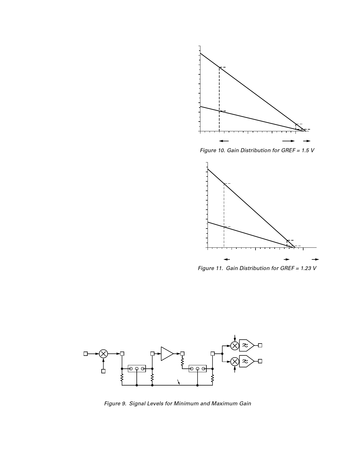
As noted earlier, the gain in dB is reduced linearly with the
voltage VG on the GAIN pin. Figure 10 shows how the mixer
and IF strip gains vary with VG when GREF is connected to VMID
(1.5 V) and a supply voltage of 3 V is used. Figure 11 shows
how these vary when GREF is connected to a 1.23 V reference.
90dB
80dB
70dB
60dB
(67.5dB)
50dB
IF GAIN
40dB
30dB
20dB
10dB
0dB
0
(21.5dB)
MIXER GAIN
(7.5dB)
(1.5dB)
0.4V
1V
1.8V 2V 2.2V
NORMAL OPERATING RANGE
Vg
Figure 10. Gain Distribution for GREF = 1.5 V
90dB
80dB
70dB
60dB
(67.5dB)
50dB
40dB
IF GAIN
30dB
20dB
(21.5dB)
MIXER GAIN
10dB
0dB
0
(7.5dB)
(1.5dB)
0.328V
1V
1.64V
NORMAL OPERATING RANGE
2V
Vg
Figure 11. Gain Distribution for GREF = 1.23 V
I
؎54mV
MAX INPUT
RFHI
؎1.3V
MAX OUTPUT
؎54mV
MAX INPUT
MXOP IFHI
IF BPF
؎560mV
MAX OUTPUT
؎154mV
MAX INPUT
IFOP DMIP
IF BPF
؎1.23V
MAX OUTPUT
IOUT
QOUT
LOIP
330⍀ 330⍀
(VMID)
Q
CONSTANT
–16dBm
(؎50mV)
(TYPICAL
IMPEDANCE)
(LOCATION OF OPTIONAL
SECOND IF FILTER)
Figure 9. Signal Levels for Minimum and Maximum Gain
–18–
REV. 0
Share Link: 