AD61009 Просмотр технического описания (PDF) - Analog Devices
Номер в каталоге
Компоненты Описание
производитель
AD61009 Datasheet PDF : 24 Pages
| |||
VPOS
AD61009
2RT
RT
IFOP
BPF
2RT
DMIP
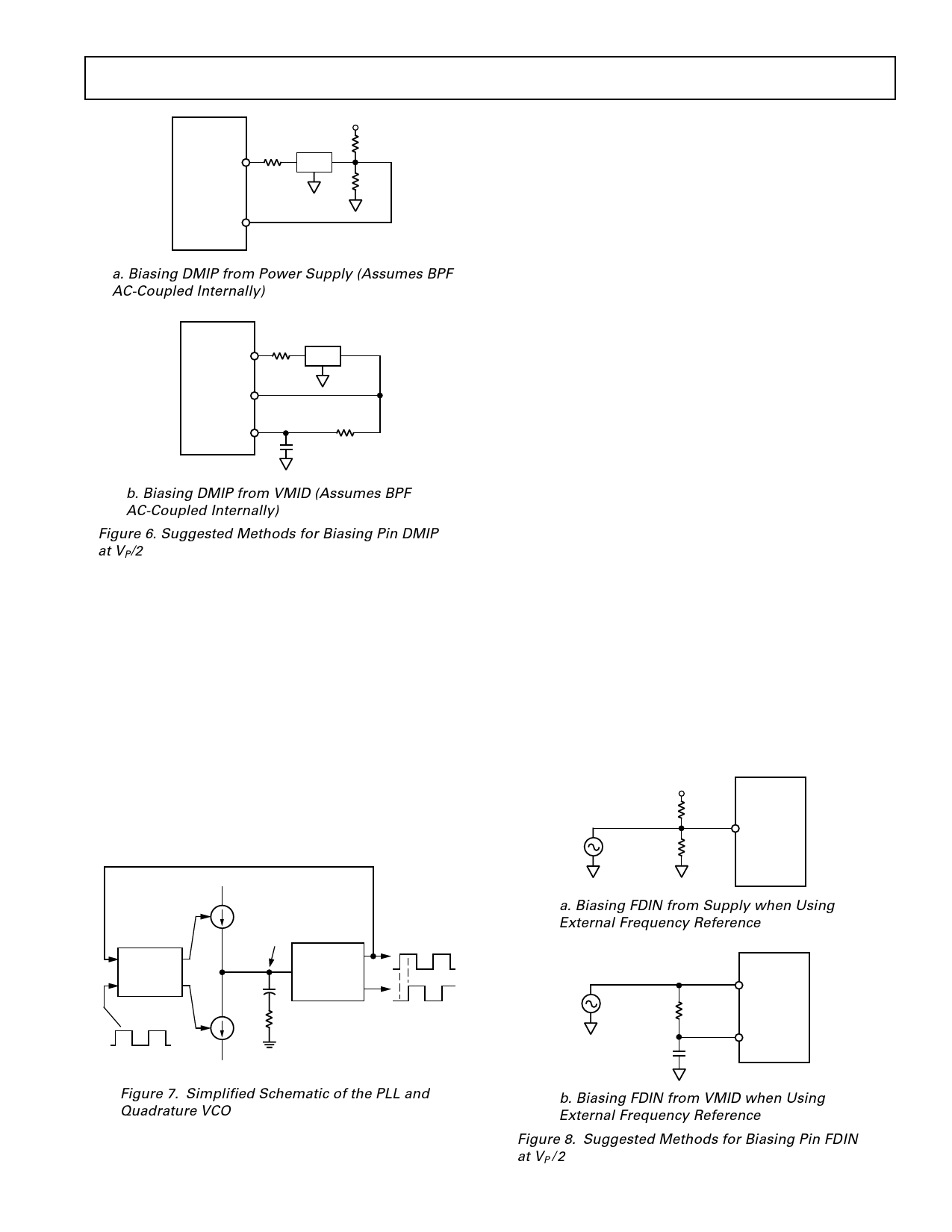
a. Biasing DMIP from Power Supply (Assumes BPF
AC-Coupled Internally)
AD61009
RT
IFOP
BPF
DMIP
VMID
RT
CBYPASS
b. Biasing DMIP from VMID (Assumes BPF
AC-Coupled Internally)
Figure 6. Suggested Methods for Biasing Pin DMIP
at VP/2
For IFs < 3 MHz, the on-chip low-pass filters (2 MHz cutoff)
do not attenuate the IF or feedthrough products; thus, the
maximum input voltage at DMIP must be limited to ± 75 mV
to allow sufficient headroom at the I and Q outputs for not only
the desired baseband signal but also the unattenuated higher-
order demodulation products. These products can be removed
by an external low-pass filter.
Phase-Locked Loop
The demodulators are driven by quadrature signals that are
provided by a variable frequency quadrature oscillator (VFQO),
phase locked to a reference signal applied to pin FDIN. When
this signal is at the IF, inphase and quadrature baseband outputs
are generated at IOUT and QOUT, respectively. The quadra-
ture accuracy of this VFQO is typically –1.2° at 10.7 MHz. The
PLL uses a sequential-phase detector that comprises low power
emitter-coupled logic and a charge pump (Figure 7).
AD61009
The reference signal may be provided from an external source,
in the form of a high-level clock, typically a low level signal
(± 400 mV) since there is an input amplifier between FDIN and
the loop’s phase detector. For example, the IF output itself can
be used by connecting DMIP to FDIN, which will then provide
automatic carrier recover for synchronous AM detection and
take advantage of any post-IF filtering. Pin FDIN must be
biased at VP/2; Figure 9 shows suggested methods.
The VFQO operates from 1 MHz to 12 MHz and is controlled by
the voltage between VPOS and FLTR. In normal operation, a
series RC network, forming the PLL loop filter, is connected
from FLTR to ground. The use of an integral sample-hold
system ensures that the frequency-control voltage on pin FLTR
remains held during power-down, so reacquisition of the carrier
typically occurs in 16.5 µs.
In practice, the probability of a phase mismatch at power-up is
high, so the worst-case linear settling period to full lock needs to
be considered in making filter choices. This is typically 16.5 µs at
an IF of 10.7 MHz for a ±100 mV signal at DMIP and FDIN.
Bias System
The AD61009 operates from a single supply, VP, usually of 3 V,
at a typical supply current of 8.5 mA at midgain and T = 27°C,
corresponding to a power consumption of 25 mW. Any voltage
from 2.85 V to 5.5 V may be used.
The bias system includes a fast-acting active-high CMOS-
compatible power-up switch, allowing the part to idle at 550 µA
when disabled. Biasing is proportional-to-absolute-temperature
(PTAT) to ensure stable gain with temperature.
An independent regulator generates a voltage at the midpoint
of the supply (VP/2) which appears at the VMID pin, at a low
impedance. This voltage does not shut down, ensuring that the
major signal interfaces (e.g., mixer-to-IF and IF-to-demodulators)
remain biased at all times, thus minimizing transient disturbances
at power-up and allowing the use of substantial decoupling
capacitors on this node. The quiescent consumption of this
regulator is included in the idling current.
VPOS
50k⍀
EXTERNAL
FREQUENCY
REFERENCE
50k⍀
AD61009
FDIN
F
SEQUENTIAL U
PHASE
R
DETECTOR D
REFERENCE CARRIER
(FDIN AFTER LIMITING)
IU~
40A
VF
VARIABLE-
FREQUENCY
QUADRATURE
C OSCILLATOR
ID~
R
40A
I-CLOCK
90؇
Q-CLOCK
(ECL OUTPUTS)
Figure 7. Simplified Schematic of the PLL and
Quadrature VCO
a. Biasing FDIN from Supply when Using
External Frequency Reference
EXTERNAL
FREQUENCY
REFERENCE
AD61009
FDIN
50k⍀
CBYPASS
VMID
b. Biasing FDIN from VMID when Using
External Frequency Reference
Figure 8. Suggested Methods for Biasing Pin FDIN
at VP / 2
REV. 0
–17–
Share Link: 