X28C010D Просмотр технического описания (PDF) - Intersil
Номер в каталоге
Компоненты Описание
производитель
X28C010D Datasheet PDF : 23 Pages
| |||
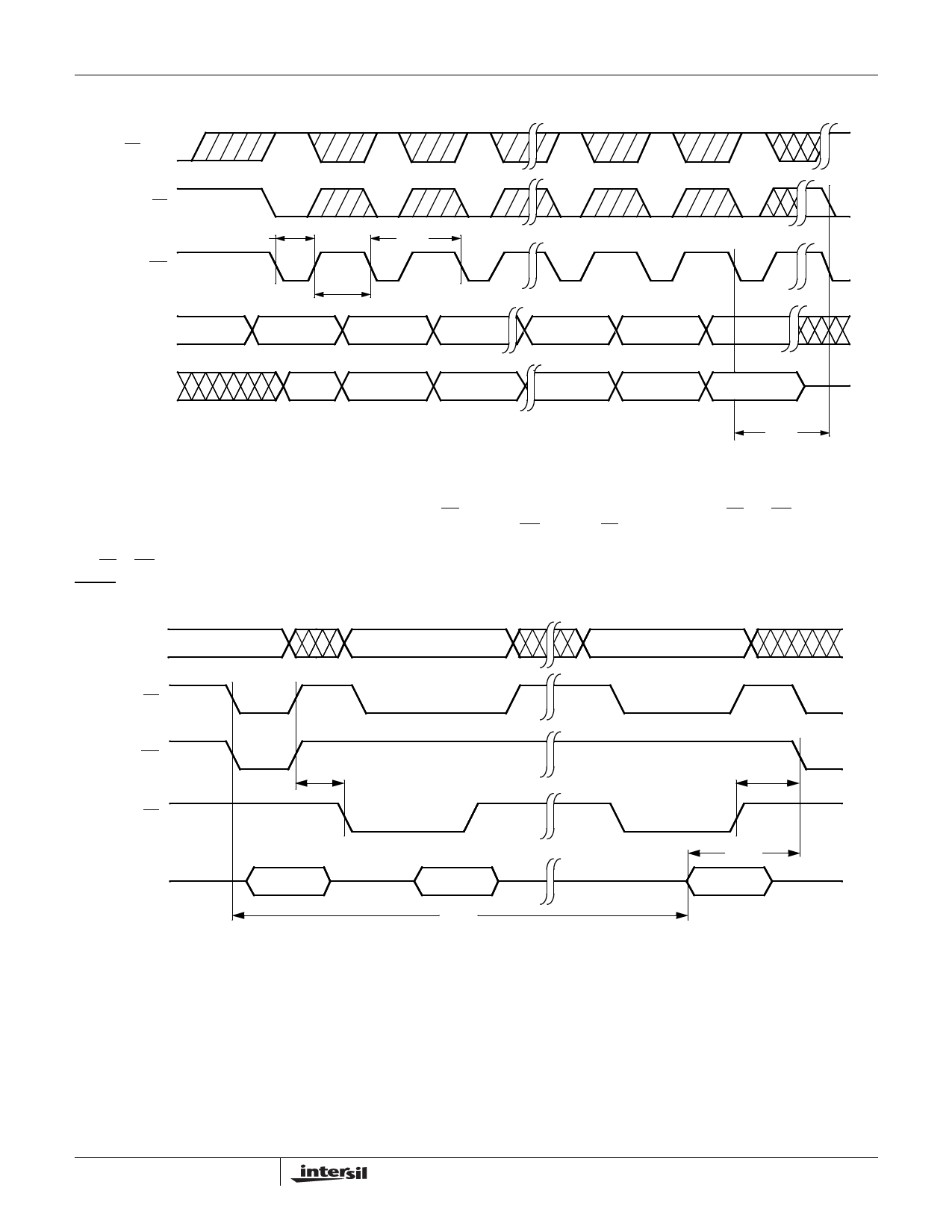
Page Write Cycle
OE (Note 5)
X28C010
CE
tWP
WE
Address* (Note 6)
tWPH
tBLC
I/O
Last Byte
Byte 0
Byte 1
Byte 2
Byte n
Byte n+1
*For each successive write within the page write operation, A8-A16 should be the same or
writes to an unknown address could occur.
Byte n+2
tWC
NOTES:
5. Between successive byte writes within a page write operation, OE can be strobed LOW: e.g. this can be done with CE and WE HIGH to fetch
data from another memory device within the system for the next write; or with WE HIGH and CE LOW effectively performing a polling operation.
6. The timings shown above are unique to page write operations. Individual byte load operations within the page write must conform to either the
CE or WE controlled write cycle timing.
DATA Polling Timing Diagram (Note 7)
Address
An
An
An
CE
WE
tOEH
OE
I/O7
DIN = X
DOUT = X
tWC
tOES
tDW
DOUT = X
14
FN8105.0
May 11, 2005
Share Link: 