WFF840B Просмотр технического описания (PDF) - Shenzhen Winsemi Microelectronics Co., Ltd
Номер в каталоге
Компоненты Описание
производитель
WFF840B Datasheet PDF : 7 Pages
| |||
Features
� 9A,500V, RDS(on)(Max0.75Ω)@VGS=10V
� Ultra-low Gate charge(Typical 28nC)
� Fast Switching Capability
� 100%Avalanche Tested
� Maximum Junction Temperature Range(150℃)
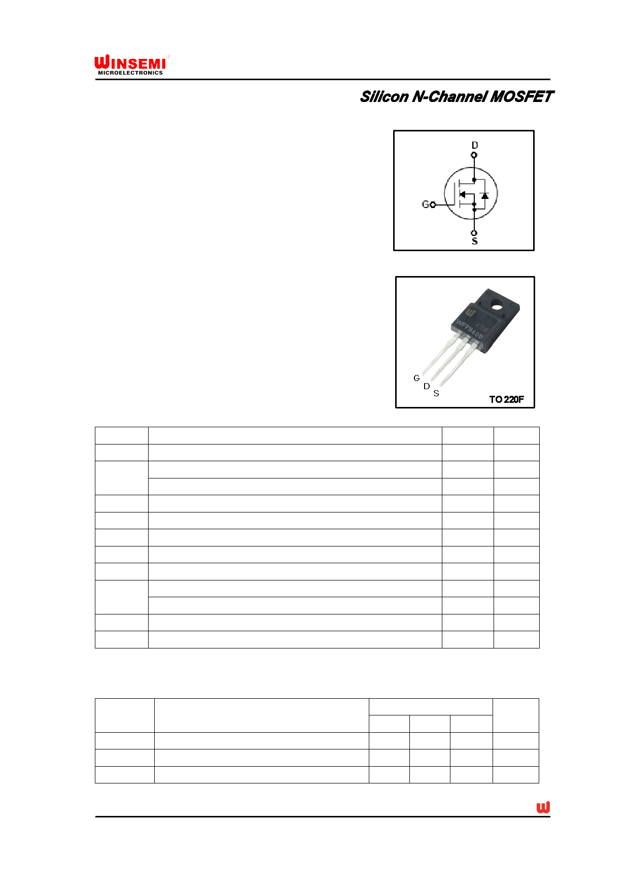
WFF840B
Silicon N-Channel MOSFET
General Description
This Power MOSFET is produced using Winsemi’s advanced
planar stripe, DMOS technology. This latest technology has been
especially designed to minimize on-state resistance, have a high
rugged avalanche characteristics. This devices is specially well
suited for high efficiency switch model power supplies, power
factor correction and half bridge and full bridge resonant topology
line a electronic lamp ballast.
Absolute Maximum Ratings
Symbol
Parameter
VDSS
ID
Drain Source Voltage
Continuous Drain Current(@Tc=25℃)
Continuous Drain Current(@Tc=100℃)
IDM
Drain Current Pulsed
VGS
Gate to Source Voltage
EAS
Single Pulsed Avalanche Energy
EAR
Repetitive Avalanche Energy
dv/dt
Peak Diode Recovery dv /dt
Total Power Dissipation(@Tc=25℃)
PD
Derating Factor above 25℃
TJ,Tstg
Junction and Storage Temperature
TL
Channel Temperature
*Drain current limited by maximum junction temperature
(Note1)
(Note2)
(Note1)
(Note3)
Value
500
9*
5.4*
36*
±30
360
13.5
4.5
135
1.07
-55~150
300
Units
V
A
A
A
V
mJ
mJ
V/ ns
W
W/℃
℃
℃
Thermal Characteristics
Symbol
Parameter
RQJC
RQCS
RQJA
Thermal Resistance , Junction -to -Case
Thermal Resistance , Case-to-Sink
Thermal Resistance , Junction-to -Ambient
Value
Min Typ Max
-
-
0.93
-
0.5
-
-
-
62.5
Units
℃/W
℃/W
℃/W
Rev.A Jul.2011
Copyright@WinSemi Co., Ltd., All right reserved.
Share Link: 