VN610SP-E Просмотр технического описания (PDF) - STMicroelectronics
Номер в каталоге
Компоненты Описание
производитель
VN610SP-E Datasheet PDF : 18 Pages
| |||
VN610SP-E
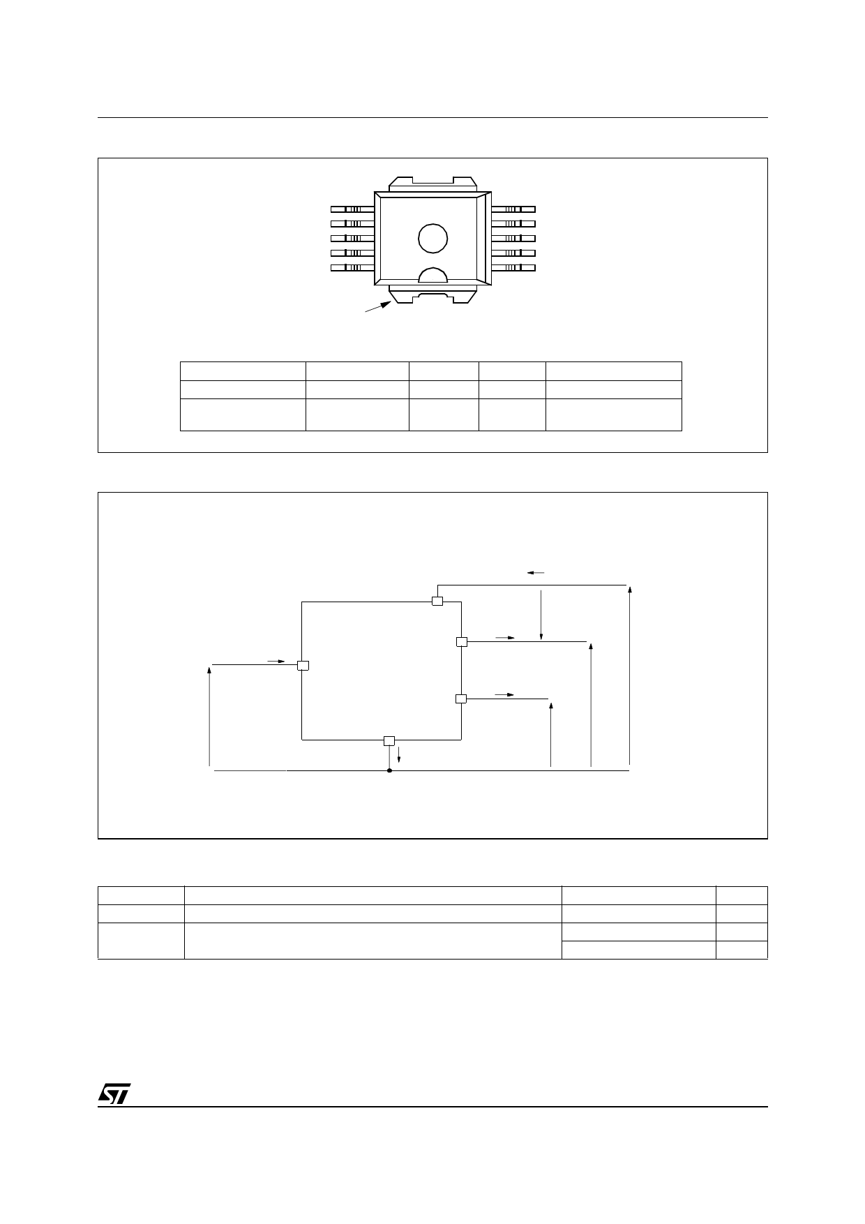
Figure 3. Configuration Diagram (Top View) & Suggested Connections for Unused and N.C. Pins
GROUND
6
5
INPUT
7
4
C.SENSE
8
3
N.C.
N.C.
9
2
10
1
11
VCC
OUTPUT
OUTPUT
OUTPUT
OUTPUT
OUTPUT
Connection / Pin
Floating
To Ground
Current Sense
Through
1KΩresistor
N.C.
X
X
Output
X
Input
X
Through 10KΩ resistor
Figure 4. Current and Voltage Conventions
IIN
VIN
VCC
INPUT
OUTPUT
CURRENT SENSE
GND
IGND
IS
VF
IOUT
VOUT
ISENSE
VSENSE
VCC
Table 4. Thermal Data
Symbol
Rthj-case
Rthj-amb
Parameter
Thermal resistance junction-case
Thermal resistance junction-ambient
(MAX)
(MAX)
Value
0.9
50.9 (1)
36(2)
Note: (1) When mounted on a standard single-sided FR-4 board with 0.5cm2 of Cu (at least 35µm thick).
Note: (2) When mounted on a standard single-sided FR-4 board with 6 cm2 of Cu (at least 35µm thick).
Unit
°C/W
°C/W
°C/W
3/18
Share Link: 