UPD77115AF1-XXX-CN6 Просмотр технического описания (PDF) - NEC => Renesas Technology
Номер в каталоге
Компоненты Описание
производитель
UPD77115AF1-XXX-CN6 Datasheet PDF : 56 Pages
| |||
µPD77115, 77115A
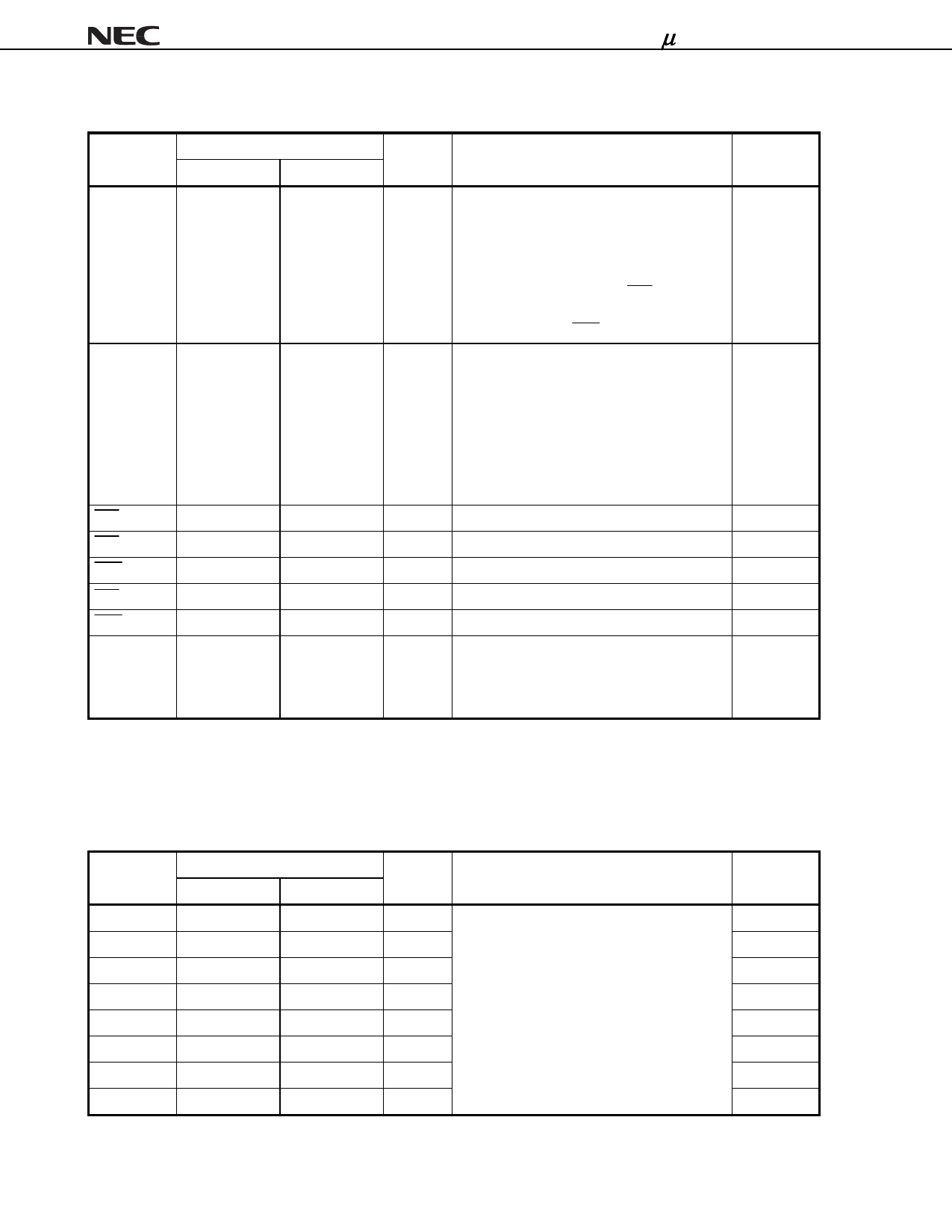
• Host interface
Pin Name
HA1
Pin No.
80-pin FBGA 80-pin TQFP
D8
56
HA0
C9
55
HCS
F9
HRD
F6
HWR
E7
HRE
G8
HWE
F7
HD0 to HD15
H8,G7,H6,J7,
F5,G6,J6,J5,
G5,F4,J4,G4,
H3,J3,G3,G2
46
47
48
44
45
41,40,36,35,
34,33,32,29,
28,27,26,25,
24,23,20,17
I/O
Function
Shared by:
Input Specifies the register to be accessed by HD15 to
−
HD0.
• 1: Accesses the host interface status
register (HST).
• 0: Accesses the host transmit data register
(HDT (out)) when read (HRD = 0), and
host receive data register (HDT (in)) when
written (HWR = 0).
Input Specifies the register to be accessed by HD15 to
−
HD0.
• 1: Accesses bits 15 to 8 of HST, HDT (in),
and HDT (out).
• 0: Accesses bits 7 to 0 of HST, HDT (in),
and HDT (out).
When 8-bit mode, this signal becomes valid.
When 16-bit mode, this signal becomes invalid.
Input Chip select input
−
Input Host read input
−
Input Host write input
−
Output Host read enable output
−
Output Host write enable output
−
I/O 16-bit host data bus
−
(3S)
Remark The pins marked “3S” under the heading “I/O” go into a high-impedance state when the host interface is
not being accessed.
• I/O ports
Pin Name
P0
P1
P2
P3
P4
P5
P6
P7
Pin No.
80-pin FBGA 80-pin TQFP
F2
16
G1
15
E4
14
F3
13
E2
11
D2
10
E1
9
D4
7
I/O
Function
I/O General-purpose I/O port
I/O
I/O
I/O
I/O
I/O
I/O
I/O
Shared by:
−
−
−
−
PLL0
PLL1
PLL2
PLL3
12
Data Sheet U14867EJ5V0DS
Share Link: 