UPD77114 Просмотр технического описания (PDF) - NEC => Renesas Technology
Номер в каталоге
Компоненты Описание
производитель
UPD77114 Datasheet PDF : 62 Pages
| |||
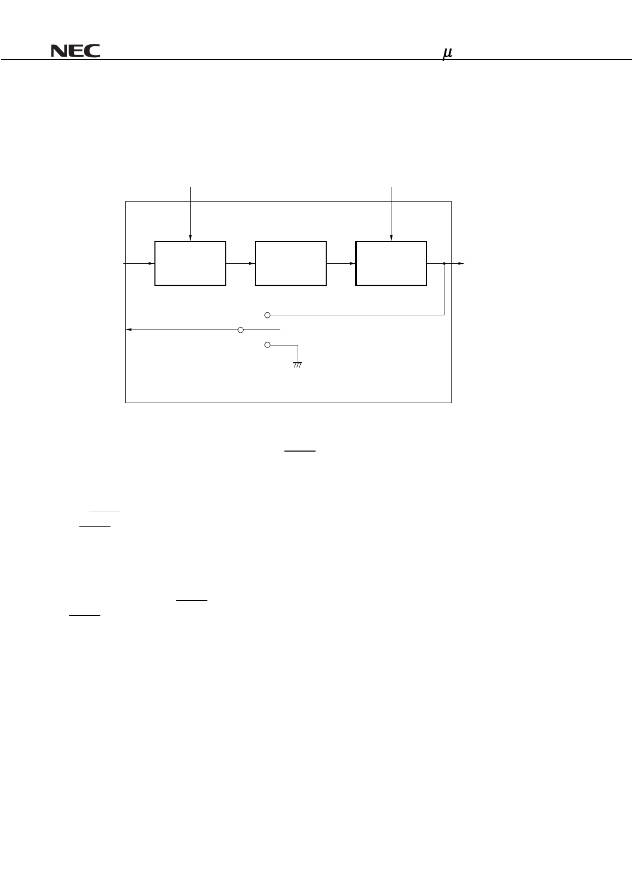
µPD77113A, 77114
3. CLOCK GENERATOR
The clock generator generates an internal system clock based on the external clock input from the CLKIN pin and
supplies the generated clock to the internal units of the DSP.
For details of how to set the PLL multiple, refer to 4.2 Initializing PLL, and 8.1 Clock Control Options.
Stop mode
Halt mode
CLKIN
CLKOUT
PLL control circuit
×m
Output divider
÷n
Halt divider
÷l
Internal
system clock
4. RESET FUNCTION
When a low level of a specified width is input to the RESET pin, the device is initialized.
4.1 Hardware Reset
If the RESET pin is asserted active (low level) for a specified period, the internal circuitry of the DSP is initialized.
If the RESET pin is then deasserted inactive (high level), boot processing of the instruction RAM is performed
according to the status of the port pins (P0 and P1). After boot processing, processing is executed starting from the
instruction at address 0x200 of instruction memory (reset entry). In addition, a self-check is performed by the internal
data RAM at the same time as the boot processing. This check takes about 20 ms (at 50 MHz operation, the length
of this period is in inverse proportion to the operating frequency.)
On power application, the RESET pin must be asserted active (low level) after 4 input clocks have been input with
the RESET pin in the inactive status (high level), after the supply voltage has reached the level of the operating
voltage. In other words, no power-ON reset function is available. On power application, the PLL must be initialized.
20
Data Sheet U14373EJ3V0DS
Share Link: 