UPD75036CW-XXX Просмотр технического описания (PDF) - NEC => Renesas Technology
Номер в каталоге
Компоненты Описание
производитель
UPD75036CW-XXX Datasheet PDF : 58 Pages
| |||
µPD75036
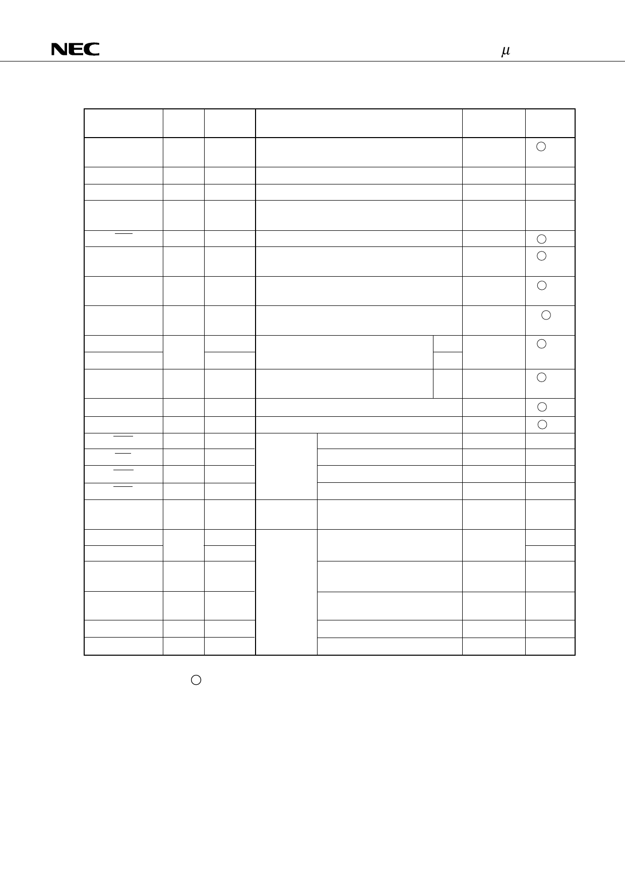
3.2 NON-PORT PINS (1/2)
Pin
TI0
PTO0
PCL
BUZ
SCK
SO/SB0
SI/SB1
INT4
INT0
INT1
INT2
KR0 - KR3
KR4-KR7
MAR
MAI
MAZ
MAT
PPO
AN0 - AN3
AN4 - AN7
AVREF+
AVREF-
AVDD
AVSS
Input/
output
Shared
pin
Function
Input
P13
Input for receiving external event pulse signal for
timer/event counter
I/O
P20
Timer/event counter output
I/O
P22
Clock output
I/O
P23
Output for arbitrary frequency output (for buzzer
output or system clock trimming)
I/O
P01
Serial clock I/O
I/O
P02
Serial data output
Serial bus I/O
I/O
P03
Serial data input
Serial bus I/O
Input
P00
Edge detection vectored interrupt input (either
rising edge or falling edge detection)
Input
P10
Edge detection vectored interrupt input
P11
(detection edge selectable)
Note 2
Note 3
Input
P12
Edge detection testable input (rising edge Note 3
detection)
I/O P60 - P63 Parallel falling edge detection testable input
I/O P70 - P73 Parallel falling edge detection testable input
I/O
P100 In MFT
Reverse integration signal output
I/O
P101
integral A/D Integration signal output
converter
I/O
P102
mode
Autozero signal output
I/O
P103
Comparator input
I/O
Input
Input
P21
In MFT timer
mode
P110 - P113 For A /D
–
converter
only
–
Timer pulse output
8-bit analog input
Reference voltage input
(on AVDD side)
Input
–
–
–
Reference voltage input
(on AVSS side)
Operating power supply
–
–
Reference GND potential
When reset
–
Input
Input
Input
Input
Input
Input
–
–
–
Input
Input
Note 4
Note 4
Note 4
Note 4
Input
Input
–
–
–
–
I/O circuit
typeNote 1
BF-C
E-B
E-B
E-B
FF-A
FF-B
MF-C
B
BF-C
BF-C
FF-A
FF-A
M
M
M
M
E-B
Y-A
Y
Z-A
Z-A
–
–
Notes 1. The circle ( ) indicates the Schmitt trigger input.
2. Clock synchronous
3. Asynchronous
4. High level (when pull-up resistors are provided) or high impedance
Remark MFT: Multifunction Timer
9
Share Link: 