ADM101EARM(1999) Просмотр технического описания (PDF) - Analog Devices
Номер в каталоге
Компоненты Описание
производитель
ADM101EARM Datasheet PDF : 6 Pages
| |||
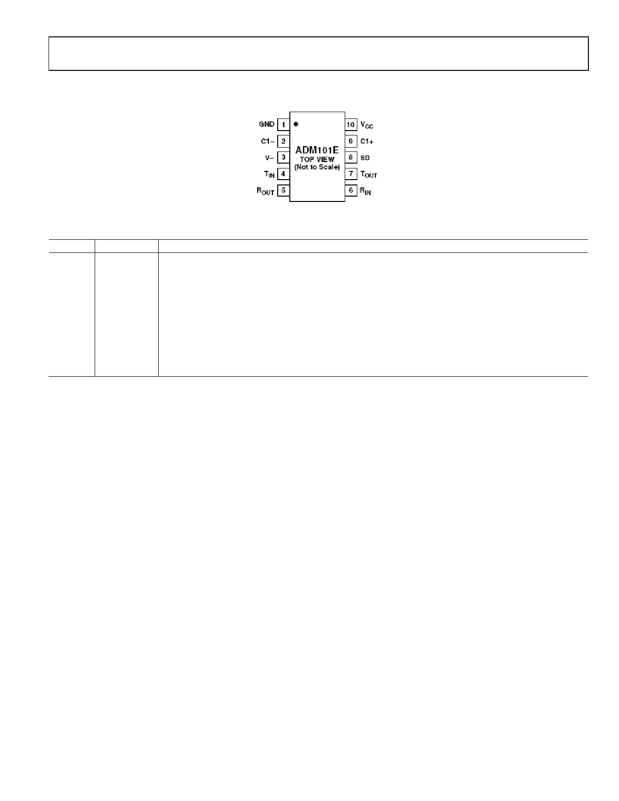
ADM101E
GENERAL DESCRIPTION
The ADM101E is an RS-232 compatible line driver/receiver in
the Analog Devices Craft Port series, containing one driver (trans-
mitter) and one receiver. It is ideal for serial communication in
small portable devices such as mobile telephones, palmtop per-
sonal computers and personal digital assistants, where a full,
RS-232 serial interface is not required, and only Tx and Rx lines
are required for low speed communication between devices. The
ADM101E operates from a single, +5 V supply, and generates
its own, on-chip, –5 V power supply, thus removing the need for
a negative power supply for the driver.
CIRCUIT DESCRIPTION
The internal circuitry consists of three main sections. These are:
1. A charge pump dc-to-dc converter.
2. 5 V logic to EIA-232 driver.
3. EIA-232 to 5 V logic receiver.
Charge Pump DC-DC Converter
The dc-dc converter generates a negative supply voltage from
the +5 V supply, thus removing the need for a separate –5 V
rail. It consists of an on-chip 200 kHz oscillator, switching ma-
trix and two external capacitors, as shown in Figure 7.
VCC
GND
S1
S3
+
S2
C1 S4
+
C2
GND
V– = –VCC
INTERNAL
OSCILLATOR
Figure 7. Charge Pump DC–DC Converter
When S1 and S2 are closed, S3 and S4 are open, and C1
charges to +VCC. S1 and S2 are then opened, while S3 and S4
are closed to connect C1 across C2, dumping charge into C2.
Since the positive terminal of C2 is at ground, a negative voltage
will be built up on its negative terminal with each cycle of the
oscillator. This voltage depends on the current drawn from C2.
If the current is small, the voltage will be close to –VCC, but will
fall as the current drawn increases.
Charge Pump Capacitors And Supply Decoupling
For proper operation of the charge pump, the capacitors should
have an equivalent series resistance (ESR) less than 1 Ω. As the
charge pump draws current pulses from VCC, the VCC decou-
pling capacitor should also have low ESR. The VCC decoupling
capacitor and V– reservoir capacitor should also have low ESR
because they determine how effectively ESD pulses are clamped
to VCC or V– by the on-chip clamp diodes. Tantalum or mono-
lithic ceramic capacitors are suitable for these components. If
using tantalum capacitors, do not forget to observe polarity.
Transmitter (Driver) Section
The driver converts 5 V logic input levels into RS-232 compat-
ible output levels. With VCC = +5 V and driving an EIA-232
load, the output voltage swing is typically ± 4.2 V.
Receiver Section
The receivers are inverting level-shifters that accept EIA-232
input levels and translate them into 5 V logic output levels.
The inputs have internal 5 kΩ pull-down resistors to ground and
are also protected against overvoltages of up to ± 25 V. The
guaranteed switching thresholds are 0.8 V minimum and 2.8 V
maximum. An unconnected receiver input is pulled to 0 V by
the internal 5 kΩ pull-down resistor. This, therefore, results in a
Logic 1 output level for unconnected inputs or for inputs con-
nected to GND.
The receivers have Schmitt trigger input with a hysteresis level
of 0.25 V. This ensures error-free reception for both noisy in-
puts and for inputs with slow transition times.
SHUTDOWN INPUT
The shutdown input allows the ADM101E to be put into an
ultralow power mode where the dc-dc converter is switched off
and the transmitter is disabled. The receiver remains active
during shutdown. Logic 0 at this input enables the ADM101E,
while a Logic 1 at this input shuts down the ADM101E.
REV. 0
–5–
Share Link: 