UAA3580 Просмотр технического описания (PDF) - Philips Electronics
Номер в каталоге
Компоненты Описание
производитель
UAA3580
Philips Electronics

UAA3580 Datasheet PDF : 24 Pages
| |||
Philips Semiconductors
Wideband code division multiple access
frequency division duplex zero IF receiver
Objective specification
UAA3580
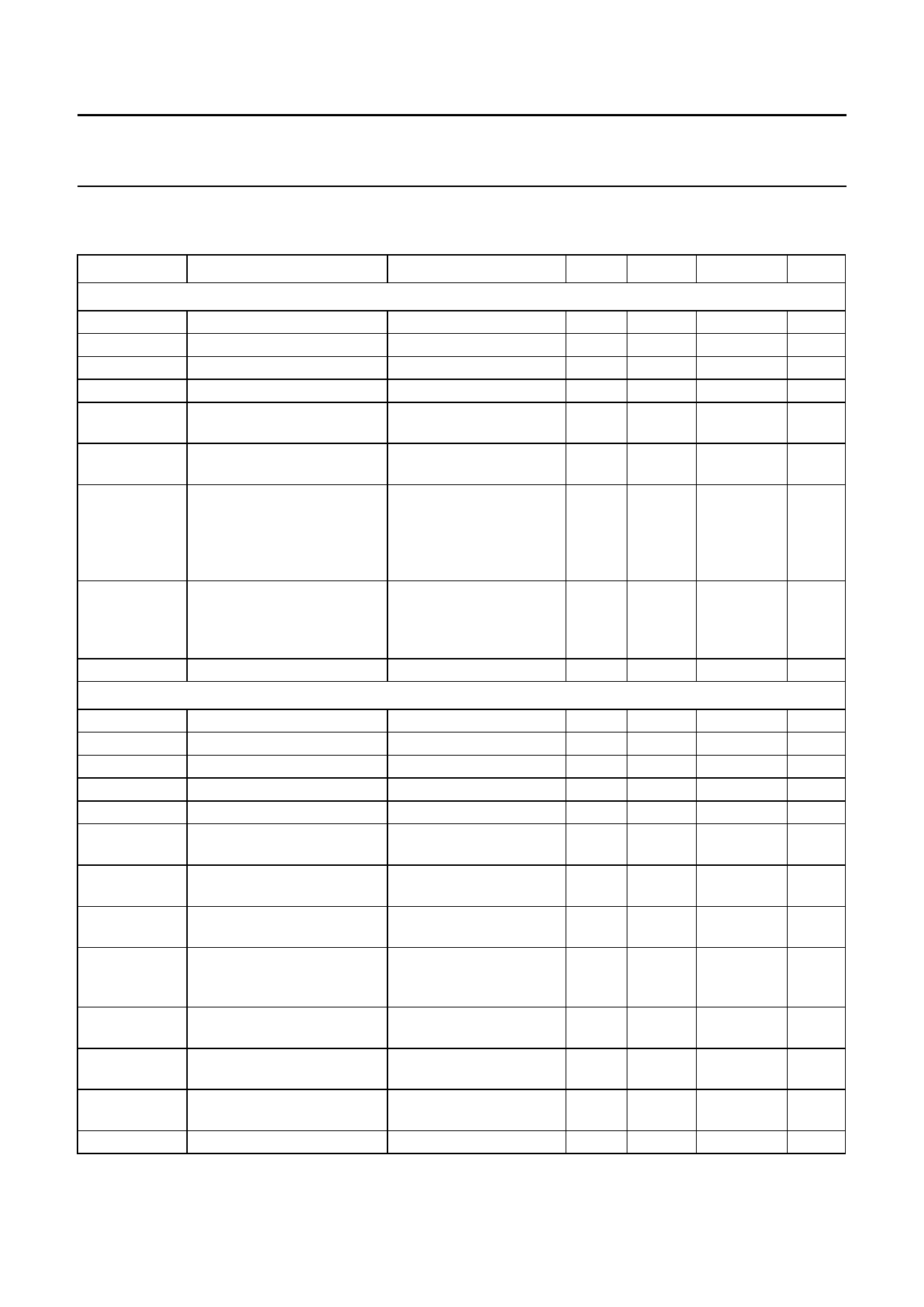
14 AC CHARACTERISTICS
VCCA = 2.6 V; Tamb = 25 °C; unless otherwise specified.
SYMBOL
PARAMETER
CONDITIONS
MIN.
RF receiver inputs; pins RFIN and RFIP
fi(RF)
RF input frequency
2.11
Ri
input resistance
−
Ci
input capacitance
−
s11
input power matching
with external balun
−
F
noise figure
in receive mode with
−
maximum gain
CP1
1 dB compression point
in receive mode with
−23
maximum gain
IP3
input referred 3rd-order
in receive mode with
−18
intercept point
maximum gain;
interference 20 MHz
away from channel
bandwidth
IP2
input referred 2nd-order
in receive mode with
37
intercept point
maximum gain;
interferers 190 MHz away
from channel bandwidth
ϕn
phase noise
at 15 MHz offset
−
Baseband IQ section; pins IP, IN, QP and QN
Gv(max)
Gv(min)
AGCtot
Gstep(AGC)
AGCtot(lin)
∆Gv(IQ)
∆Φ
Vo(max)
Io(max)
Voffset(diff)
HP−3dB
LP−3dB
∆d(g)
maximum voltage gain
minimum voltage gain
total AGC range
AGC gain step
total AGC linearity
voltage gain mismatch
between the I and Q paths
quadrature phase error
between the I and Q paths
maximum output voltage per
pin
maximum output current per
pin
differential output offset
voltage
−3 dB high-pass corner
frequency
−3 dB low-pass corner
frequency
group delay variation
peak error
RL(diff) = 10 kΩ;
THD < 3%
Vo(p-p) = 1.75 V at 1 MHz;
RL(diff) = 10 kΩ;
CL(diff) = 20 pF
2nd-order high-pass
frequency
5th-order low-pass
frequency
100 kHz < fo < 2 MHz
92
12
−
−
−0.5
−
−
0.75
650
−20
10
2.25
−
TYP.
−
170
1
−10
3.2
−20
−15
42
−
96
17
79
1
−
−
−
−
−
−
15
2.4
260
MAX.
2.17
−
−
−
4
−
−
−
−135
100
22
−
−
+0.5
0.5
5
−
−
+20
20
2.55
−
UNIT
GHz
Ω
pF
dB
dB
dBm
dBm
dBm
dBc/Hz
dB
dB
dB
dB
dB
dB
deg
V
µA
mV
kHz
MHz
ns
2002 Oct 30
15
Share Link: