TDA8760K/4/C1 Просмотр технического описания (PDF) - Philips Electronics
Номер в каталоге
Компоненты Описание
производитель
TDA8760K/4/C1 Datasheet PDF : 28 Pages
| |||
Philips Semiconductors
10-bit high-speed analog-to-digital
converter
Product specification
TDA8760
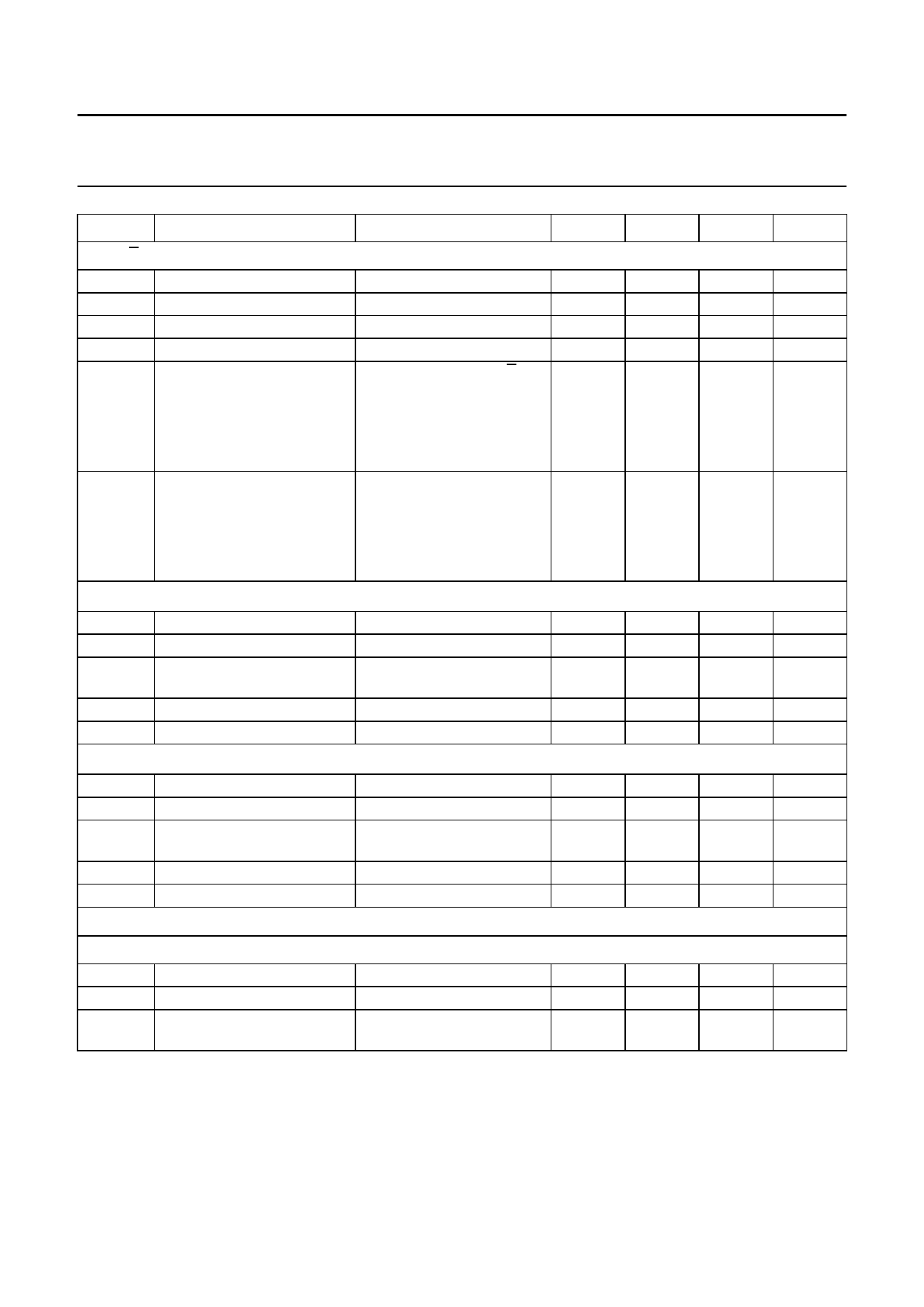
SYMBOL
PARAMETER
CONDITIONS
MIN.
TYP.
MAX.
VI AND VI (REFERENCED TO AGND); see also Tables 1 and 2
IIL
IIH
ZI
CI
VIoffset(d)
LOW level input current
HIGH level input current
input impedance
input capacitance
input offset voltage
VrefH − VrefL = 1.5 V
−
VrefH − VrefL = 1.5 V
−
fi = 4.43 MHz
−
fi = 4.43 MHz
−
differential mode; VI = VI;
output code 511; Table 1
7
−
22
−
2
−
4.5
−
VIoffset(s) input offset voltage
VCCA = 5 V
3.3
3.4
3.6
VCCA = 4.75 V
3.2
−
3.45
VCCA = 5.25 V
3.3
−
3.8
single mode; VI = VIoffset(s);
output code 511; Table 2
VCCA = 5 V
VCCA = 4.75 V
VCCA = 5.25 V
3.6
3.7
3.8
3.5
−
3.65
3.6
−
4.0
Voltage controlled regulator inputs VrefH and VrefL (referenced to AGND); differential input
VrefH
VrefL
VI(p-p)
reference voltage HIGH
reference voltage LOW
input voltage amplitude
(peak-to-peak value)
4.0
4.5
VCCA
2.5
3.0
3.5
1.4
1.5
1.6
IrefH
input current at VrefH
IrefL
input current at VrefL
−
10
−
−
10
−
Voltage controlled regulator inputs VrefH and VrefL (referenced to AGND); single input
VrefH
VrefL
VI(p-p)
reference voltage HIGH
reference voltage LOW
input voltage amplitude
(peak-to-peak value)
4.0
4.4
VCCA
2.5
3.0
3.5
1.3
1.4
1.5
IrefH
input current at VrefH
IrefL
input current at VrefL
−
10
−
−
10
−
Outputs (referenced to DGND)
DIGITAL OUTPUTS D9 TO D0 AND IR (REFERENCED TO DGND)
VOL
LOW level output voltage
IO = 2 mA
VOH
HIGH level output voltage IO = −0.4 mA
IO
output current in 3-state
0.4 V < VO < VCCO
mode
0
−
2.4
−
−20
−
0.4
VCCD
+20
UNIT
µA
µA
kΩ
pF
V
V
V
V
V
V
V
V
V
µA
µA
V
V
V
µA
µA
V
V
µA
1996 Sep 12
9
Share Link: 