SX1231 Просмотр технического описания (PDF) - Semtech Corporation
Номер в каталоге
Компоненты Описание
производитель
SX1231 Datasheet PDF : 81 Pages
| |||
SX1231
ADVANCED COMMUNICATIONS & SENSING
DATASHEET
3.4.5. Modulation Shaping
Modulation shaping can be applied in both OOK and FSK modulation modes, to improve the narrowband response of the
transmitter. Both shaping features are controlled with PaRamp bits in RegPaRamp.
In FSK mode, a Gaussian filter with BT = 0.3, 0.5 or 1 is used to filter the modulation stream, at the input of the sigma-
delta modulator. If the Gaussian filter is enabled when the SX1231 is in Continuous mode, DCLK signal on pin 10
(DIO1/DCLK) will trigger an interrupt on the uC each time a new bit has to be transmitted. Please refer to section 5.4.2
for details.
When OOK modulation is used, the PA bias voltages are ramped up and down smoothly when the PA is turned on and
off, to reduce spectral splatter.
Note the transmitter must be restarted if the PaRamp setting is changed, in order to recalibrate the built-in filter.
3.4.6. Power Amplifiers
Three power amplifier blocks are embedded in the SX1231. The first one, herein referred to as PA0, can generate up to
+13 dBm into a 50 Ohm load. PA0 shares a common front-end pin RFIO (pin 21) with the receiver LNA.
PA1 and PA2 are both connected to pin PA_BOOST (pin 23), allowing for two distinct power ranges:
A low power mode, where -18 dBm < Pout < 13 dBm, with PA1 enabled
A higher power mode, when PA1 and PA2 are combined, providing up to +17 dBm to a matched load.
When PA1 and PA2 are combined to deliver +17 dBm to the antenna, a specific impedance matching / harmonic filtering
design is required to ensure impedance transformation and regulatory compliance.
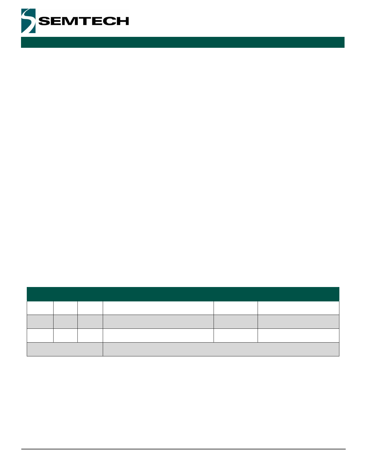
All PA settings are controlled by RegPaLevel, and the truth table of settings is given in Table 10.
Table 10 Power Amplifier Mode Selection Truth Table
Pa0On Pa1On Pa2On
Mode
Power Range
1
0
0
PA0 output on pin RFIO
-18 to +13 dBm
0
1
0
PA1 enabled on pin PA_BOOST
-18 to +13 dBm
0
1
1
PA1 and PA2 combined on pin PA_BOOST -14 to +17 dBm
Other combinations
Reserved
Pout Formula
-18 dBm + OutputPower
-18 dBm + OutputPower
-14 dBm + OutputPower
Notes - To ensure correct operation at the highest power levels, please make sure to adjust the Over Current Protection
Limit accordingly in RegOcp.
- If PA_BOOST pin is not used (+13dBm applications and less), the pin can be left floating.
3.4.7. Over Current Protection
An over current protection block is built-in the chip. It helps preventing surge currents required when the transmitter is used
at its highest power levels, thus protecting the battery that may power the application. The current clamping value is
controlled by OcpTrim bits in RegOcp, and is calculated with the following formula:
Imax = 45 + 5 × OcpTrim(mA)
Rev 3 - April 2010
Page 21
www.semtech.com
Share Link: 