SST39VF088 Просмотр технического описания (PDF) - Silicon Storage Technology
Номер в каталоге
Компоненты Описание
производитель
SST39VF088 Datasheet PDF : 22 Pages
| |||
8 Mbit Multi-Purpose Flash
SST39VF088
Preliminary Specifications
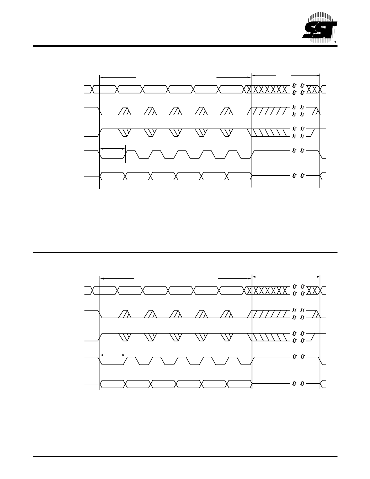
Six-Byte Code for Block-Erase
TBE
ADDRESS AMS-0
AAA
555
AAA
AAA
555
BAX
CE#
OE#
WE#
TWP
DQ7-0
AA
SW0
55
SW1
80
SW2
AA
SW3
55
SW4
30
SW5
Note: The device also supports CE# controlled Block-Erase operation.
The WE# and CE# signals are interchangeable as long as minimum timings are met. (See Table 10)
AMS = Most significant address
AMS = A19 for SST39VF088
1227 F08.2
FIGURE 8: WE# CONTROLLED BLOCK-ERASE TIMING DIAGRAM
Six-byte Code for Sector-Erase
TSE
ADDRESS AMS-0
AAA
555
AAA
AAA
555
SAX
CE#
OE#
WE#
TWP
DQ7-0
AA
SW0
55
SW1
80
SW2
AA
SW3
55
SW4
50
SW5
Note: The device also supports CE# controlled Sector-Erase operation.
The WE# and CE# signals are interchangeable as long as minimum timings are met. (See Table 10)
AMS = Most significant address
AMS = A19 for SST39VF088
FIGURE 9: WE# CONTROLLED SECTOR-ERASE TIMING DIAGRAM
1227 F09.2
©2003 Silicon Storage Technology, Inc.
13
S71227-04-000
11/03
Share Link: 