PLL102-03 Просмотр технического описания (PDF) - PhaseLink Corporation
Номер в каталоге
Компоненты Описание
производитель
PLL102-03 Datasheet PDF : 6 Pages
| |||
PLL102-03
Low Skew Output Buffer
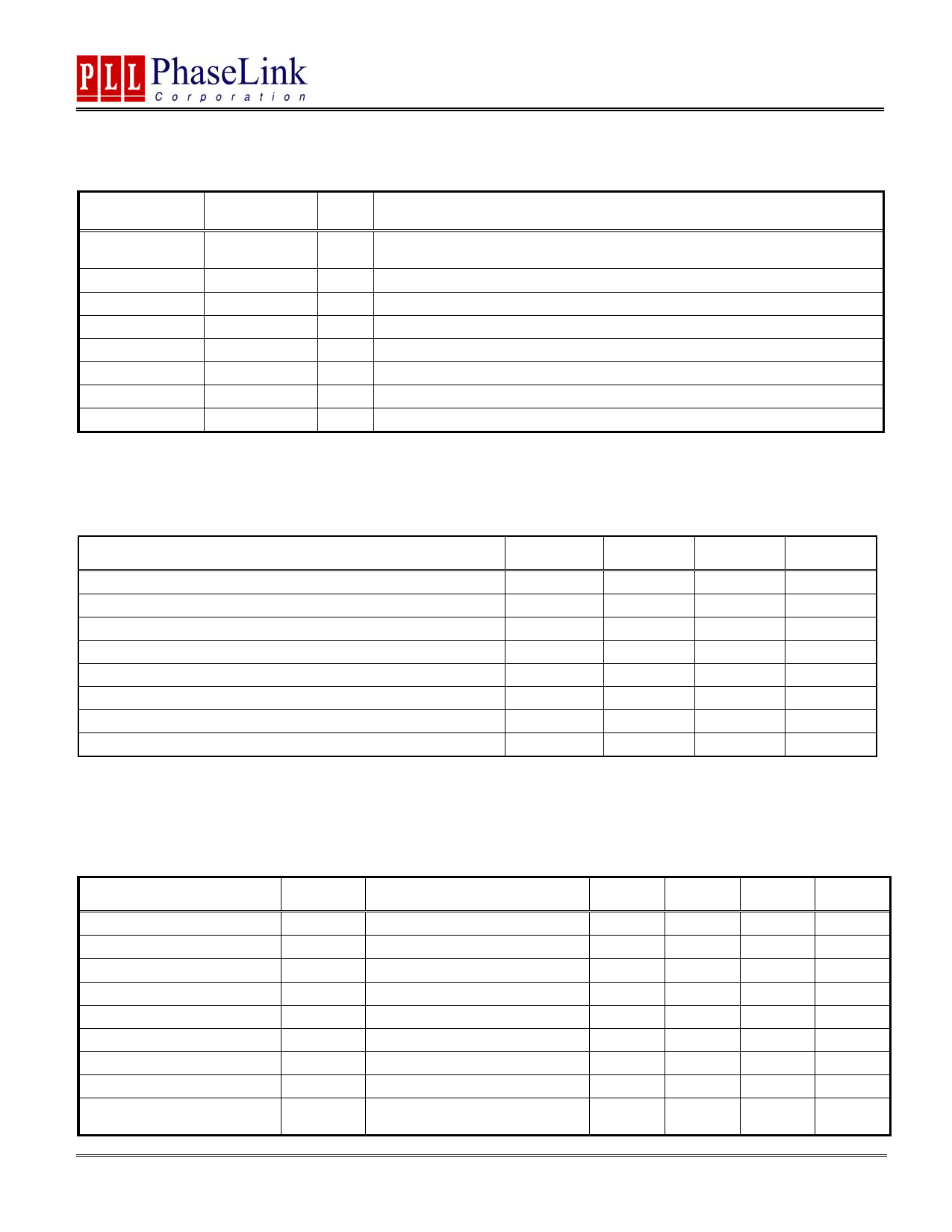
PIN DESCRIPTIONS
Name
Number Type
Description
REF1
CLK22
CLK12
GND
CLK32
VDD
CLK42
CLKOUT2
1
I
Input reference frequency. Spread spectrum modulation on this signal will be
passed to the output (up to 100kHz SST modulation).
2
O Buffered clock output.
3
O Buffered clock output.
4
P Ground.
5
O Buffered clock output.
6
P 3.3V Power Supply.
7
O Buffered clock output.
8
O Buffered clock output. Internal feed back on this pin.
Notes: 1: Weak pull-down. 2: Weak pull-down on all outputs.
ELECTRICAL SPECIFICATIONS
1. Absolute Maximum Ratings
PARAMETERS
SYMBOL
MIN.
MAX.
UNITS
Supply Voltage
Input Voltage, dc
Output Voltage, dc
Storage Temperature
Ambient Operating Temperature*
Junction Temperature
Lead Temperature (soldering, 10s)
ESD Protection, Human Body Model
VDD
4.6
V
VI
-0.5
VDD+0.5
V
VO
-0.5
VDD+0.5
V
TS
-65
150
°C
TA
-40
85
°C
TJ
125
°C
260
°C
2
kV
Exposure of the device under conditions beyond the limits specified by Maximum Ratings for extended periods may cause permanent damage to the
device and affect product reliability. These conditions represent a stress rating only, and functional operations of the device at these or any other con-
ditions above the operational limits noted in this specification is not implied.
* Note: Operating Temperature is guaranteed by design for all parts (COMMERCIAL and INDUSTRIAL), but tested for COMMERCIAL grade only.
2. Electrical Characteristics
PARAMETERS
Supply Voltage
Input Low Voltage
Input High Voltage
Input Low Current
Input High Current
Output Low Voltage
Output High Voltage
Power Down Supply Current
Supply Current
SYMBOL
CONDITIONS
VDD
VIL
VIH
IIL
VIN = 0V
IIH
VIN = VDD
VOL
IOL = 50mA
VOH
IOH = 50mA
IDD
REF = 0MHz
IDD
Unloaded outputs at 133MHz,
SEL inputs at VDD or GND
MIN.
2.97
2.0
2.4
TYP.
19
0.10
0.25
2.9
0.3
35
MAX.
3.63
0.8
50.0
100.0
0.4
50.0
45
UNITS
V
V
V
µA
µA
V
V
µA
mA
47745 Fremont Blvd., Fremont, California 94538 Tel (510) 492-0990 Fax (510) 492-0991 www.phaselink.com Rev 02/23/06 Page 2
Share Link: 