PCF2119VU Просмотр технического описания (PDF) - Philips Electronics
Номер в каталоге
Компоненты Описание
производитель
PCF2119VU Datasheet PDF : 68 Pages
| |||
Philips Semiconductors
LCD controllers/drivers
Product specification
PCF2119X
8 INSTRUCTIONS
Only two PCF2119x registers, the Instruction Register (IR)
and the Data Register (DR) can be directly controlled by
the MPU. Before internal operation, control information is
stored temporarily in these registers, to allow interfacing to
various types of MPUs which operate at different speeds
or to allow interface to peripheral control ICs. The
PCF2119x operation is controlled by the instructions
shown in Table 6 together with their execution time.
Details are explained in subsequent sections.
Instructions are of 4 types, those that:
1. Designate PCF2119x functions such as display
format, data length, etc.
2. Set internal RAM addresses
3. Perform data transfer with internal RAM
4. Others.
In normal use, category 3 instructions are used most
frequently. However, automatic incrementing by 1
(or decrementing by 1) of internal RAM addresses after
each data write lessens the MPU program load. The
display shift in particular can be performed concurrently
with display data write, enabling the designer to develop
systems in minimum time with maximum programming
efficiency.
During internal operation, no instructions other than the
‘read busy flag’ and ‘read address’ instructions will be
executed. Because the busy flag is set to a logic 1 while an
instruction is being executed, check to ensure it is a logic 0
before sending the next instruction or wait for the
maximum instruction execution time, as given in Table 6.
An instruction sent while the busy flag is logic 1 will not be
executed.
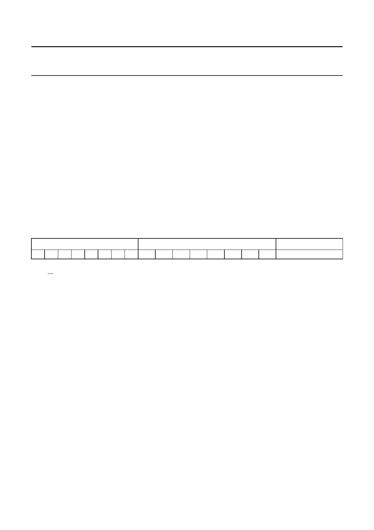
Table 5 Instruction set for I2C-bus commands
CONTROL BYTE
COMMAND BYTE
I2C-BUS COMMANDS
Co RS 0 0 0 0 0 0 DB7 DB6 DB5 DB4 DB3 DB2 DB1 DB0 note 1
Note
1. R/W is set together with the slave address.
2003 Jan 30
22
Share Link: 