HI5746KCBZ Просмотр технического описания (PDF) - Intersil
Номер в каталоге
Компоненты Описание
производитель
HI5746KCBZ Datasheet PDF : 16 Pages
| |||
HI5746
at positive full scale when the VIN+ input is at
VDC + 0.25V and the VIN- input is at VDC - 0.25V (VIN+ -
VIN- = +0.5V). Conversely, the converter will be at
negative fullscale when the VIN+ input is equal to VDC -
0.25V and VIN- is at VDC + 0.25V (VIN+ - VIN- = -0.5V).
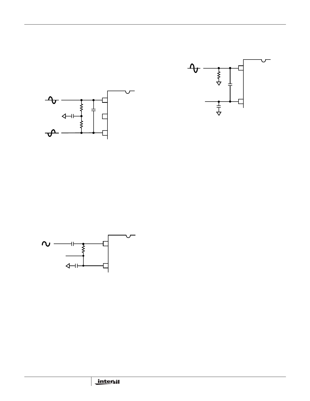
The analog input can be DC coupled (Figure 27) as long as
the inputs are within the analog input common mode voltage
range (0.25V ≤ VDC ≤ 4.75V).
VIN
VDC
VDC
-VIN
VIN+
R
C
HI5746
VDC
R
VIN-
FIGURE 27. DC COUPLED DIFFERENTIAL INPUT
The resistors, R, in Figure 27 are not absolutely necessary
but may be used as load setting resistors. A capacitor, C,
connected from VIN+ to VIN- will help filter any high
frequency noise on the inputs, also improving performance.
Values around 20pF are sufficient and can be used on AC
coupled inputs as well. Note, however, that the value of
capacitor C chosen must take into account the highest
frequency component of the analog input signal.
Analog Input, Single-Ended Connection
The configuration shown in Figure 28 may be used with a
single ended AC coupled input.
VIN
VDC
VIN+
R
HI5746
VIN-
FIGURE 28. AC COUPLED SINGLE ENDED INPUT
Again, assume the difference between VREF+, typically 2.5V,
and VREF-, typically 2V, is 0.5V. If VIN is a 1VP-P sinewave,
then VIN+ is a 1VP-P sinewave riding on a positive voltage
equal to VDC. The converter will be at positive full scale
when VIN+ is at VDC + 0.5V (VIN+ - VIN- = +0.5V) and will
be at negative full scale when VIN+ is equal to
VDC - 0.5V (VIN+ - VIN- = -0.5V). Sufficient headroom must
be provided such that the input voltage never goes above
+5V or below AGND. In this case, VDC could range between
0.5V and 4.5V without a significant change in ADC
performance. The simplest way to produce VDC is to use the
DC bias source, VDC, output of the HI5746.
The single ended analog input can be DC coupled
(Figure 27) as long as the input is within the analog input
common mode voltage range.
VIN
VDC
VIN+
R
C
HI5746
VDC
VIN-
FIGURE 29. DC COUPLED SINGLE ENDED INPUT
The resistor, R, in Figure 29 is not absolutely necessary but
may be used as a load setting resistor. A capacitor, C,
connected from VIN+ to VIN- will help filter any high
frequency noise on the inputs, also improving performance.
Values around 20pF are sufficient and can be used on AC
coupled inputs as well. Note, however, that the value of
capacitor C chosen must take into account the highest
frequency component of the analog input signal.
A single ended source may give better overall system
performance if it is first converted to differential before
driving the HI5746.
Digital Output Control and Clock Requirements
The HI5746 provides a standard high-speed interface to
external TTL logic families.
In order to ensure rated performance of the HI5746, the duty
cycle of the clock should be held at 50% ±5%. It must also
have low jitter and operate at standard TTL levels.
Performance of the HI5746 will only be guaranteed at
conversion rates above 1 MSPS. This ensures proper
performance of the internal dynamic circuits. Similarly, when
power is first applied to the converter, a maximum of 20
cycles at a sample rate above 1 MSPS will have to be
performed before valid data is available.
A Data Format Select (DFS) pin is provided which will
determine the format of the digital data outputs. When at
logic low, the data will be output in offset binary format.
When at logic high, the data will be output in two’s
complement format. Refer to Table 1 for further information.
13
Share Link: 