HI5767/4CB(2000) Просмотр технического описания (PDF) - Intersil
Номер в каталоге
Компоненты Описание
производитель
HI5767/4CB Datasheet PDF : 13 Pages
| |||
HI5767
Signal To Noise and Distortion Ratio (SINAD)
SINAD is the ratio of the measured RMS signal to RMS sum
of all the other spectral components below the Nyquist
frequency, fS/2, excluding DC.
Signal To Noise Ratio (SNR)
SNR is the ratio of the measured RMS signal to RMS noise at
a specified input and sampling frequency. The noise is the
RMS sum of all of the spectral components below fS/2
excluding the fundamental, the first five harmonics and DC.
Total Harmonic Distortion (THD)
THD is the ratio of the RMS sum of the first 5 harmonic
components to the RMS value of the fundamental input signal.
2nd and 3rd Harmonic Distortion
This is the ratio of the RMS value of the applicable harmonic
component to the RMS value of the fundamental input signal.
Spurious Free Dynamic Range (SFDR)
SFDR is the ratio of the fundamental RMS amplitude to the
RMS amplitude of the next largest spectral component in the
spectrum below fS/2.
Intermodulation Distortion (IMD)
Nonlinearities in the signal path will tend to generate
intermodulation products when two tones, f1 and f2, are
present at the inputs. The ratio of the measured signal to the
distortion terms is calculated. The terms included in the
calculation are (f1+f2), (f1-f2), (2f1), (2f2), (2f1+f2), (2f1-f2),
(f1+2f2), (f1-2f2). The ADC is tested with each tone 6dB
below full scale.
Transient Response
Transient response is measured by providing a full-scale
transition to the analog input of the ADC and measuring the
number of cycles it takes for the output code to settle within
10-bit accuracy.
Over-Voltage Recovery
Over-Voltage Recovery is measured by providing a full-scale
transition to the analog input of the ADC which overdrives
the input by 200mV, and measuring the number of cycles it
takes for the output code to settle within 10-bit accuracy.
Full Power Input Bandwidth (FPBW)
Full power input bandwidth is the analog input frequency at
which the amplitude of the digitally reconstructed output has
decreased 3dB below the amplitude of the input sine wave.
The input sine wave has an amplitude which swings from
-FS to +FS. The bandwidth given is measured at the
specified sampling frequency.
Video Definitions
Differential Gain and Differential Phase are two commonly
found video specifications for characterizing the distortion of
a chrominance signal as it is offset through the input voltage
range of an ADC.
Differential Gain (DG)
Differential Gain is the peak difference in chrominance
amplitude (in percent) relative to the reference burst.
Differential Phase (DP)
Differential Phase is the peak difference in chrominance
phase (in degrees) relative to the reference burst.
Timing Definitions
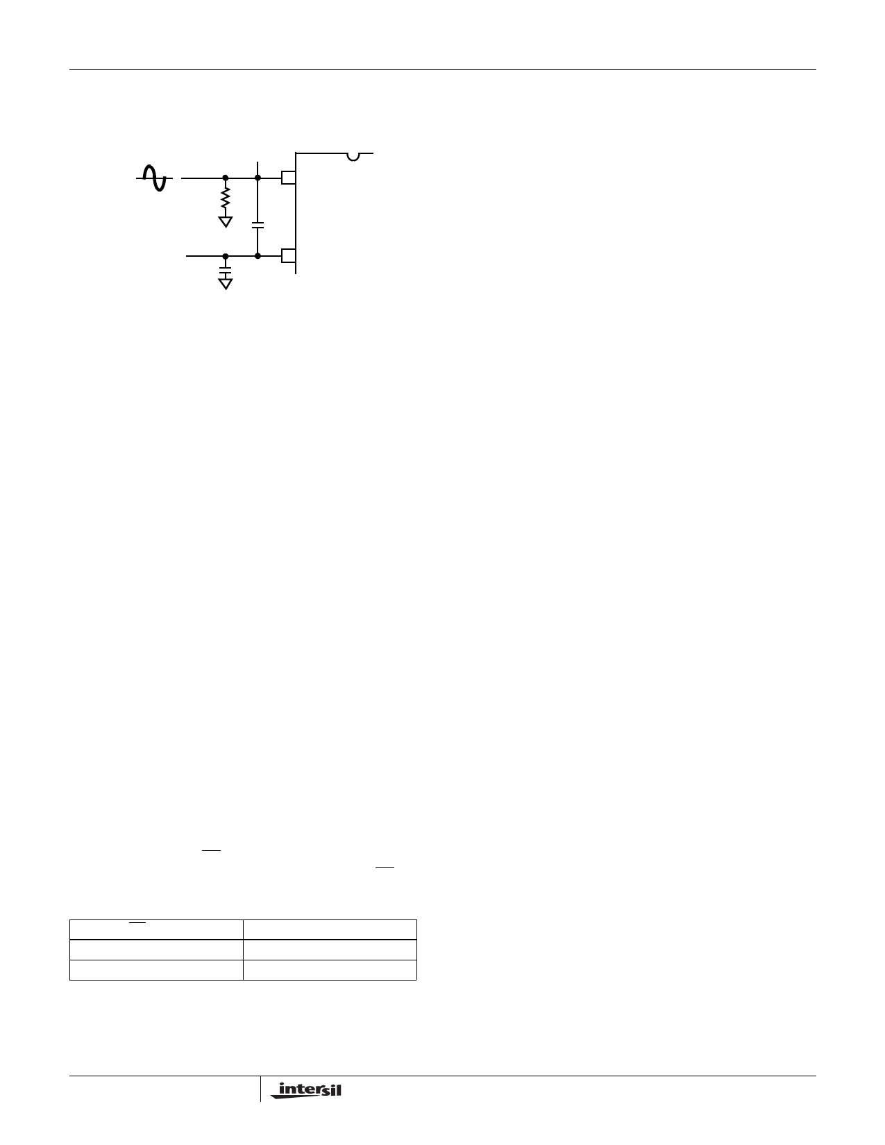
Refer to Figure 1 and Figure 2 for these definitions.
Aperture Delay (tAP)
Aperture delay is the time delay between the external
sample command (the falling edge of the clock) and the time
at which the signal is actually sampled. This delay is due to
internal clock path propagation delays.
Aperture Jitter (tAJ)
Aperture jitter is the RMS variation in the aperture delay due
to variation of internal clock path delays.
Data Hold Time (tH)
Data hold time is the time to where the previous data (N - 1)
is no longer valid.
Data Output Delay Time (tOD)
Data output delay time is the time to where the new data (N)
is valid.
Data Latency (tLAT)
After the analog sample is taken, the digital data representing
an analog input sample is output to the digital data bus on
the 7th cycle of the clock after the analog sample is taken.
This is due to the pipeline nature of the converter where the
analog sample has to ripple through the internal subconverter
stages. This delay is specified as the data latency. After the
data latency time, the digital data representing each
succeeding analog sample is output during the following
clock cycle. The digital data lags the analog input sample by 7
sample clock cycles.
Power-Up Initialization
This time is defined as the maximum number of clock cycles
that are required to initialize the converter at power-up. The
requirement arises from the need to initialize the dynamic
circuits within the converter.
All Intersil semiconductor products are manufactured, assembled and tested under ISO9000 quality systems certification.
Intersil semiconductor products are sold by description only. Intersil Corporation reserves the right to make changes in circuit design and/or specifications at any time with-
out notice. Accordingly, the reader is cautioned to verify that data sheets are current before placing orders. Information furnished by Intersil is believed to be accurate and
reliable. However, no responsibility is assumed by Intersil or its subsidiaries for its use; nor for any infringements of patents or other rights of third parties which may result
from its use. No license is granted by implication or otherwise under any patent or patent rights of Intersil or its subsidiaries.
For information regarding Intersil Corporation and its products, see web site www.intersil.com
13
Share Link: 