HI5728/6IN(1999) Просмотр технического описания (PDF) - Intersil
Номер в каталоге
Компоненты Описание
производитель
HI5728/6IN Datasheet PDF : 17 Pages
| |||
HI5728
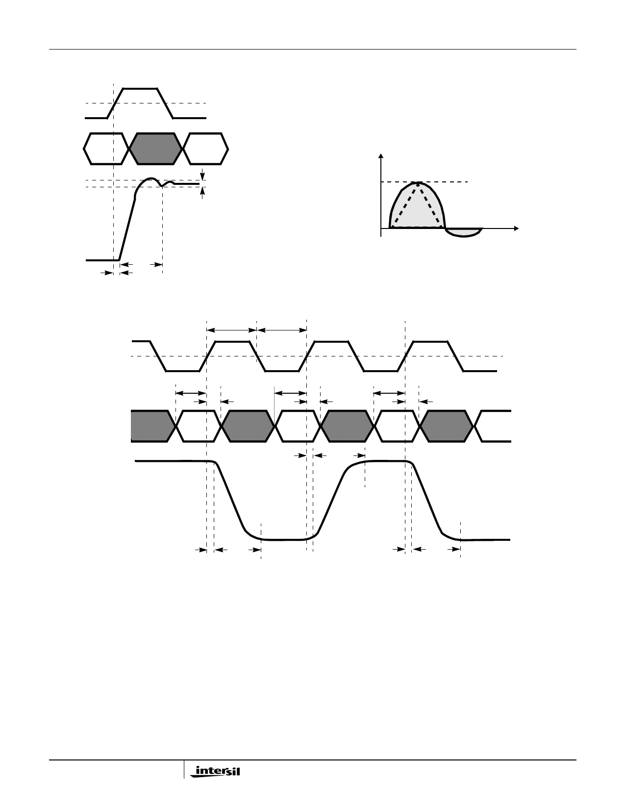
Full Scale Gain Error, is the error from an ideal ratio of 32
between the output current and the full scale adjust current
(through RSET).
Full Scale Gain Drift, is measured by setting the data inputs to
all ones and measuring the output voltage through a known
resistance as the temperature is varied from TMIN to TMAX. It is
defined as the maximum deviation from the value measured at
room temperature to the value measured at either TMIN or
TMAX. The units are ppm of FSR (full scale range) per oC.
Total Harmonic Distortion, THD, is the ratio of the DAC output
fundamental to the RMS sum of the first five harmonics.
Spurious Free Dynamic Range, SFDR, is the amplitude
difference from the fundamental to the largest harmonically or
non-harmonically related spur within the specified window.
Output Voltage Compliance Range, is the voltage limit
imposed on the output. The output impedance load should
be chosen such that the voltage developed does not violate
the compliance range.
Offset Error, is measured by setting the data inputs to all
zeros and measuring the output voltage through a known
resistance. Offset error is defined as the maximum deviation
of the output current from a value of 0mA.
Offset Drift, is measured by setting the data inputs to all zeros
and measuring the output voltage through a known resistance
as the temperature is varied from TMIN to TMAX. It is defined
as the maximum deviation from the value measured at room
temperature to the value measured at either TMIN or TMAX.
The units are ppm of FSR (Full Scale Range) per oC.
Power Supply Rejection, is measured using a single power
supply. Its nominal +5V is varied ±10% and the change in the
DAC full scale output is noted.
Reference Input Multiplying Bandwidth, is defined as the
3dB bandwidth of the voltage reference input. It is measured
by using a sinusoidal waveform as the external reference
with the digital inputs set to all 1s. The frequency is
increased until the amplitude of the output waveform is 0.707
of its original value.
Internal Reference Voltage Drift, is defined as the
maximum deviation from the value measured at room
temperature to the value measured at either TMIN or TMAX.
The units are ppm per oC.
Detailed Description
The HI5728 is a dual, 10-bit, current out, CMOS, digital to
analog converter. Its maximum update rate is 125MSPS and
can be powered by either single or dual power supplies in
the recommended range of +3V to +5V. It consumes less
than 330mW of power when using a +5V supply with the
data switching at 100MSPS. The architecture is based on a
segmented current source arrangement that reduces glitch
by reducing the amount of current switching at any one time.
The five MSBs are represented by 31 major current sources
of equivalent current. The five LSBs are comprised of binary
weighted current sources. Consider an input waveform to the
converter which is ramped through all the codes from 0 to
1023. The five LSB current sources would begin to count up.
When they reached the all high state (decimal value of 31)
and needed to count to the next code, they would all turn off
and the first major current source would turn on. To continue
counting upward, the 5 LSBs would count up another 31
codes, and then the next major current source would turn on
and the five LSBs would all turn off. The process of the
single, equivalent, major current source turning on and the
five LSBs turning off each time the converter reaches
another 31 codes greatly reduces the glitch at any one
switching point. In previous architectures that contained all
binary weighted current sources or a binary weighted
resistor ladder, the converter might have a substantially
larger amount of current turning on and off at certain, worst-
case transition points such as mid-scale and quarter scale
transitions. By greatly reducing the amount of current
switching at certain ‘major’ transitions, the overall glitch of
the converter is dramatically reduced, improving settling
times and transient problems.
Digital Inputs And Termination
The HI5728 digital inputs are guaranteed to CMOS levels.
However, TTL compatibility can be achieved by lowering the
supply voltage to 3V due to the digital threshold of the input
buffer being approximately half of the supply voltage. The
internal register is updated on the rising edge of the clock. To
minimize reflections, proper termination should be
implemented. If the lines driving the clock(s) and digital
inputs are 50Ω lines, then 50Ω termination resistors should
be placed as close to the converter inputs as possible.
Ground Plane(s)
If separate digital and analog ground planes are used, then all
of the digital functions of the device and their corresponding
components should be over the digital ground plane and
terminated to the digital ground plane. The same is true for the
analog components and the analog ground plane. Refer to the
Application Note on the HI5728 Evaluation Board for further
discussion of the ground plane(s) upon availability.
Noise Reduction
To minimize power supply noise, 0.1µF capacitors should be
placed as close as possible to the converter’s power supply
pins, AVDD and DVDD. Also, should the layout be designed
using separate digital and analog ground planes, these
capacitors should be terminated to the digital ground for
DVDD and to the analog ground for AVDD. Additional filtering
of the power supplies on the board is recommended. See
the Application Note on the HI5728 Evaluation Board for
more information upon availability.
Voltage Reference
The internal voltage reference of the device has a nominal
value of +1.2V with a ±60 ppm/oC drift coefficient over the full
16
Share Link: 