MT9074 Просмотр технического описания (PDF) - Mitel Networks
Номер в каталоге
Компоненты Описание
производитель
MT9074 Datasheet PDF : 122 Pages
| |||
MT9074
Advance Information
successive read/write operations to the HDLC FIFO
is required.
Table 13 associates the MT9074 control and status
pages with access and page descriptions.
Identification Code
The MT9074 shall be identified by the code
10101111, read from the identification code status
register (page 03H, address 1FH).
ST-BUS Streams
In T1 mode, there is one control and one status ST-
BUS stream that can be used to program / access
channel associated signalling nibbles. CSTo contains
the received channel associated signalling bits, and
for those channels whose Per Time Slot Control word
bit 1 "RPSIG" is set low, CSTi is used to control the
transmit channel associated signalling. The DSTi
and DSTo streams contain the transmit and receive
voice and digital data. Only 24 of the 32 ST-BUS
channels are used for each of DSTi, DSTo, CSTi and
CSTo. In each case individual channel mapping is as
illustrated in Table , “Table 6 - STBUS vs. DS1 to
Channel Relationship(T1),” on page 14.
In E1 mode, the ST-BUS stream can also be used to
access channel associated signalling nibbles. CSTo
contains the received channel associated signalling
bits (e.g., ITU-T R1 and R2 signalling),and for those
channels whose Per Time Slot Control word bit 1
"RPSIG" is set low, CSTi is used to control the
transmit channel associated signalling. The DSTi
and DSTo streams contain the transmit and receive
voice and digital data.
Only 30 of the 32 ST-BUS channels are used for
each of DSTi, DSTo, CSTi and CSTo. In each case
individual channel mapping is as illustrated in Table
10 Time slot to Channel Relationship.
Reset Operation (Initialization)
The MT9074 can be reset using the hardware
RESET pin (see pin description for external reset
circuit requirements) for T1 and (pin 11 in PLCC, pin
84 in MQFP) or the software reset bit RST (page 1H,
address 1AH) for E1/T1. When the device emerges
from its reset state it will begin to function with the
default settings described in Table 14 (T1) and Table
15 (E1), all control registers default to 00H. A reset
operation takes 1 full frame (125 us) to complete.
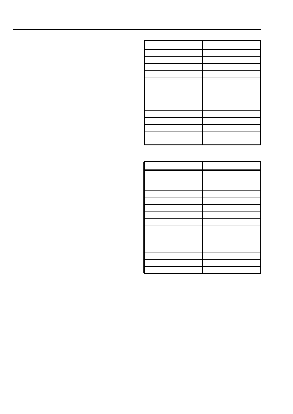
Function
Mode
Loopbacks
SLC-96
Zero Coding
Line Codes
Data Link
Signalling
AB/ABCD Bit
Debounce
Interrupts
Error Insertion
HDLC0,1
Counters
Transmit Data
Status
D4
Deactivated
Deactivated
Deactivated
Deactivated
Serial Mode
CAS Registers
Deactivated
masked
Deactivated
Deactivated
Cleared
All Ones
Table 14 - Reset Status(T1)
Function
Status
Mode
Loopbacks
Transmit FAS
Transmit non-FAS
Transmit MFAS (CAS)
Data Link
CRC Interworking
Signalling
ABCD Bit Debounce
Interrupts
RxMF Output
Error Insertion
HDLCs
Counters
Transmit Data
Termination
Deactivated
Cn0011011
1/Sn1111111
00001111
Deactivated
Activated
CAS Registers
Deactivated
Masked
Signalling Multiframe
Deactivated
Deactivated
Cleared
All Ones
Table 15 - Reset Status(E1)
Transmit Data All Ones (TxAO)
Operation
The TxAO (Transmit all ones) pin allows the PRI
interface to transmit an all ones signal from the point
of power-up without writing to any control registers.
During this time the IRQ pin is tristated. After the
interface has been initialized normal operation can
take place by making TxAO high.
20
Share Link: 