AD7818AR Просмотр технического описания (PDF) - Analog Devices
Номер в каталоге
Компоненты Описание
производитель
AD7818AR Datasheet PDF : 20 Pages
| |||
CONVST
BUSY
tPOWER-UP
t1
t3
AD7816/AD7817/AD7818
CS
OTI
RD/ WR
t15
t16
SCLK
DIN
DOUT
DB7 – DB0
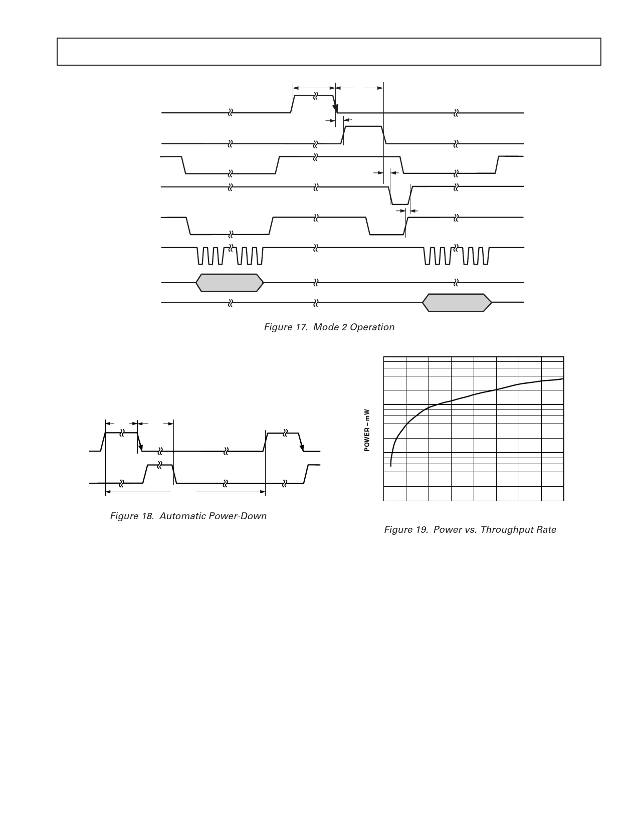
Figure 17. Mode 2 Operation
DB7(DB9) – DB0
POWER VS. THROUGHPUT
Superior power performance can be achieved by using the Auto-
matic Power-Down (Mode 2) at the end of a conversion (see
Operating Modes section of this data sheet).
CONVST
tPOWER-UP tCONVERT
2s
8s
BUSY
tCYCLE
100s @ 10kSPS
Figure 18. Automatic Power-Down
Figure 18 shows how the Automatic Power-Down is imple-
mented to achieve the optimum power performance from the
AD7816, AD7817, and AD7818. The devices are operated in
Mode 2 and the duration of CONVST pulse is set to be equal to
the power-up time (2 µs). As the throughput rate of the device is
reduced the device remains in its power-down state longer, and
the average power consumption over time drops accordingly.
For example, if the AD7817 is operated in a continuous sam-
pling mode with a throughput rate of 10 kSPS, the power con-
sumption is calculated as follows. The power dissipation during
normal operation is 4.8 mW, VDD = 3 V. If the power up time is
2 µs and the conversion time is 9 µs, the AD7817 can be said to
dissipate 4.8 mW typically for 11 µs (worst case) during each
conversion cycle. If the throughput rate is 10 kSPS, the cycle
time is 100 µs and the power dissipated while powered up dur-
ing each cycle is (11/100) × (4.8 mW) = 528 µW typ. Power
dissipated while powered down during each cycle is (89/100) ×
(3 V × 2 µA) = 5.34 µW typ. Overall power dissipated is 528 µW
+ 5.34 µW = 533 µW.
10
1
0.1
0.01
0
10 20 30 40 50
60 70 80
THROUGHPUT – kHz
Figure 19. Power vs. Throughput Rate
AD7817 SERIAL INTERFACE
The serial interface on the AD7817 is a 5-wire interface with
read and write capabilities, with data being read from the output
register via the DOUT line and data being written to the control
register via the DIN line. The part operates in a slave mode and
requires an externally applied serial clock to the SCLK input to
access data from the data register or write to the control byte.
The RD/WR line is used to determine whether data is being
written to or read from the AD7817. When data is being written
to the AD7817, the RD/WR line is set logic low and when data
is being read from the part the line is set logic high (see Figure
20). The serial interface on the AD7817 is designed to allow the
part to be interfaced to systems that provide a serial clock that is
synchronized to the serial data, such as the 80C51, 87C51,
68HC11, 68HC05, and PIC16Cxx microcontrollers.
REV. C
–15–
Share Link: 