ML674001 Просмотр технического описания (PDF) - Oki Electric Industry
Номер в каталоге
Компоненты Описание
производитель
ML674001 Datasheet PDF : 24 Pages
| |||
OKI Semiconductor
FEDL674001-01
ML674001/67Q4002/67Q4003
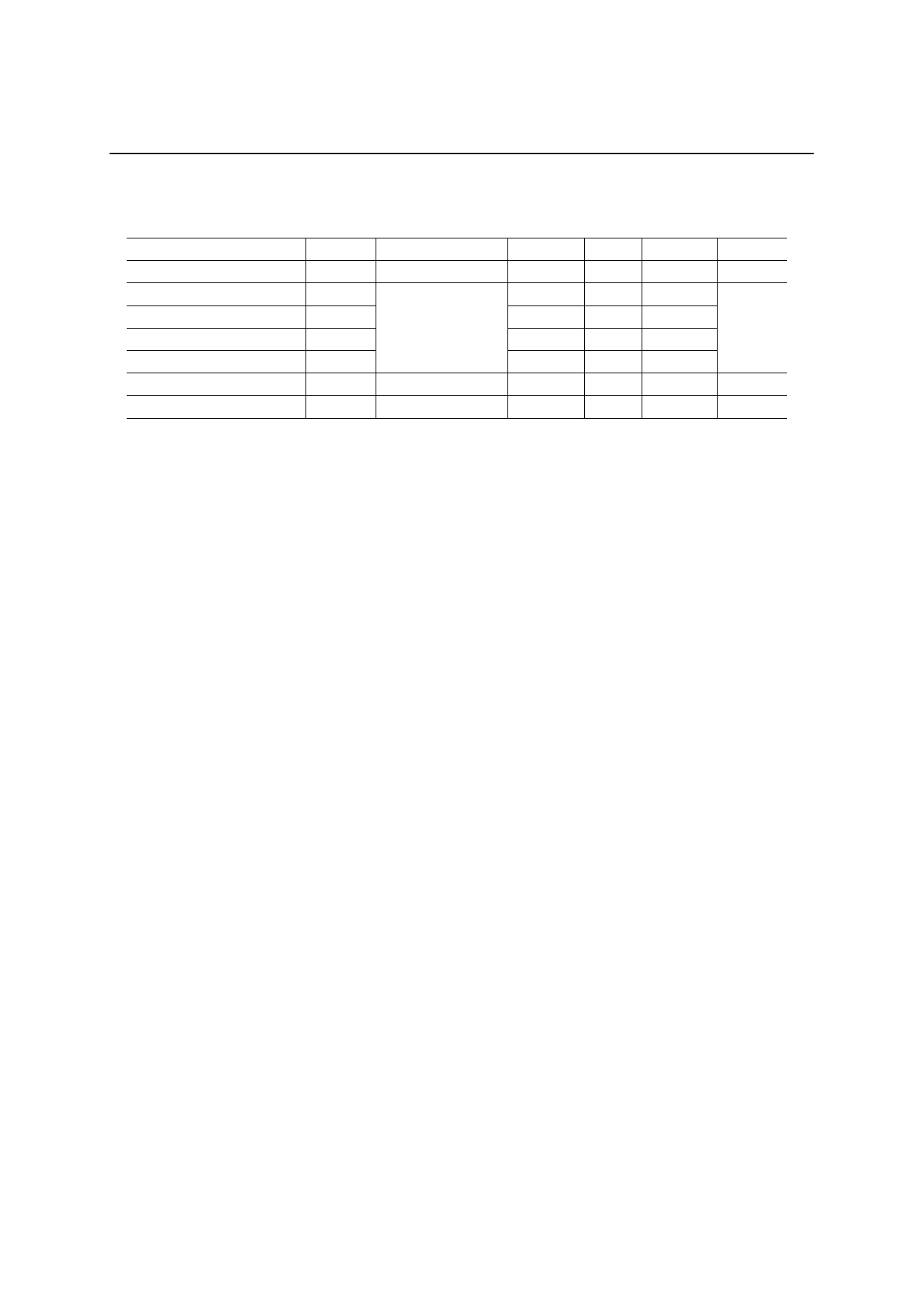
Analog-to-Digital Converter Characteristics
(VDD_CORE = 2.50 V, VDD_IO = 3.3 V, Ta = 25°C)
Item
Symbol
Conditions
Minimum Typical Maximum Unit
Resolution
n
—
—
—
10
bit
Linearity error
EL
—
±3
—
Differential linearity error
Analog input
ED
source impedance
—
±3
—
LSB
Zero scale error
EZS
Ri ≤ 1kΩ
—
±3
—
Full scale error
EFS
—
±3
—
Conversion time
tCONV
—
5
—
—
µs
Throughput
—
10
—
200
kHz
Notes: VDD_IO and AVDD should be supplied separately
• Definition of Terms
(1) Resolution: Minimum input analog value recognized. For 10-bit resolution, this is (VREF –
Aground) ÷ 1024.
(2) Linearity error: Difference between the theoretical and actual conversion characteristics.
(Note that it does not include quantization error.) The theoretical conversion characteristic
divides the voltage range between VREF and AGND into 1024 equal steps.
(3) Differential linearity error: Difference between the theoretical and actual input voltage
change producing a 1-bit change in the digital output anywhere within the conversion range.
This is an indicator of conversion characteristic smoothness. The theoretical value is (VREF –
Aground) ÷ 1024.
(4) Zero scale error: Difference between the theoretical and actual conversion characteristics at
the point where the digital output switches from “0x000” to “0x001.”
(5) Full scale error: Difference between the theoretical and actual conversion characteristics at
the point where the digital output switches from “0x3FE” to “0x3FF.”
21/24
Share Link: 