LTC1044A(Rev0) Просмотр технического описания (PDF) - Linear Technology
Номер в каталоге
Компоненты Описание
производитель
LTC1044A Datasheet PDF : 12 Pages
| |||
LTC1044A
APPLICATI S I FOR ATIO
Battery Splitter
A common need in many systems is to obtain (+) and
(–) supplies from a single battery or single power supply
system. Where current requirements are small, the circuit
shown in Figure 9 is a simple solution. It provides sym-
metrical ± output voltages, both equal to one half input
voltage. The output voltages are both referenced to pin 3
+
VB
12V
1
2
C1 3
10µF 4
LTC1044A
8
+VB/2 (6V)
7
6
REQUIRED FOR VB < 6V
5
+VB/2 (–6V)
LTC1044A • F09
C2
10µF
OUTPUT
COMMON
Figure 9. Battery Splitter
(output common). If the input voltage between pin 8 and
pin 5 is less than 6V, pin 6 should also be connected to
pin 3 as shown by the dashed line.
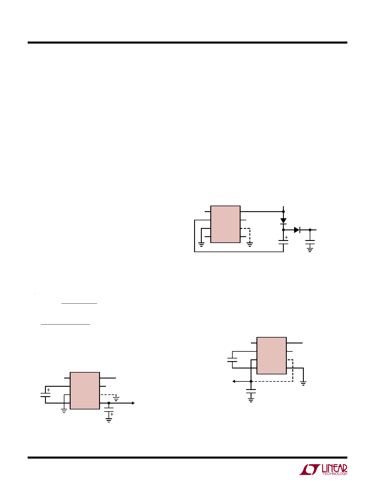
Paralleling for Lower Output Resistance
Additional flexibility of the LTC1044A is shown in Figures
10 and 11.
Figure 10 shows two LTC1044As connected in parallel to
provide a lower effective output resistance. If, however,
the output resistance is dominated by 1/(f × C1), increas-
ing the capacitor size (C1) or increasing the frequency will
be of more benefit than the paralleling circuit shown.
Figure 11 makes use of “stacking” two LTC1044As to
provide even higher voltages. A negative voltage doubler
or tripler can be achieved, depending upon how pin 8 of the
second LTC1044A is connected, as shown schematically
by the switch. The available output current will be dictated/
decreased by the product of the individual power conver-
sion efficiencies and the voltage step-up ratio.
V+
C1
10µF
1
8
2
7
3 LTC1044A 6
4
5
C1
10µF
1
8
2
7
3 LTC1044A 6
4
5
VOUT = –(V+)
1/4 CD4077
*
LTC1044A • F10
C2
20µF
*THE EXCLUSIVE NOR GATE SYNCHRONIZES BOTH LTC1044As TO MINIMIZE RIPPLE
Figure 10. Paralleling for Lower Output Resistance
V+
FOR VOUT = –3V+
FOR VOUT = –2V+
1
8
2
7
10µF 3 LTC1044A 6
4
5
10µF 1
+2
3
– (V+)
4
10µF
8
7
LTC1044A 6
5
LTC1044A • F11
VOUT
10µF
Figure 11. Stacking for Higher Voltage
8
Share Link: 