LC651432F Просмотр технического описания (PDF) - SANYO -> Panasonic
Номер в каталоге
Компоненты Описание
производитель
LC651432F Datasheet PDF : 39 Pages
| |||
Continued from preceding page.
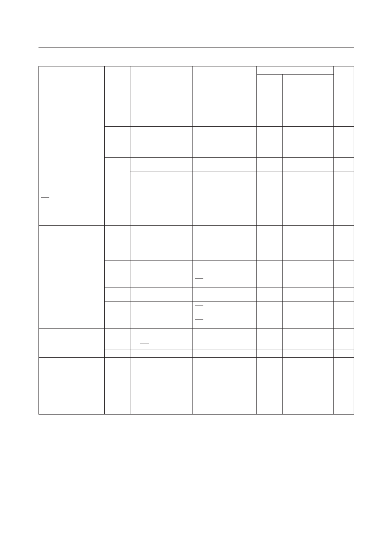
LC651432N/F/L, 651431N/F/L
Parameter
Symbol
Conditions
Applicable pins
Oscillator characteristics
Ceramic oscillator
Oscillator frequency
Oscillator stabilization time*8
Two-pin RC oscillator
Oscillator frequency
Built-in pull-up resistor I/O ports
RES
External reset characteristics
Reset time
Pin capacitance
Serial clock
Input clock cycle time
Output clock cycle time
Input clock low-level pulse
width
Output clock low-level pulse
width
Input clock high-level pulse
width
Output clock high-level pulse
width
Serial input
Data setup time
Data hold time
Serial output
Output delay time
fCFOSC*7
tCFS
fMOSC
RPP
Ru
• Figure 3, fo = 400 kHz
• Figure 3, fo = 800 kHz
• Figure 3, fo = 1 MHz
• Figure 3, fo = 4 MHz,
divide-by-three or divide-
by-four circuit used.
OSC1, OSC2
OSC1, OSC2
OSC1, OSC2
OSC1, OSC2
• Figure 4, fo = 400 kHz
• Figure 4, fo = 800 kHz,
1 MHz, or 4 MHz, divide-
by-three or divide-by-four
circuit used.
• Figure 2, Cext = 220 pF ±5%
• Figure 2, Rext = 6.8 kΩ ±1% OSC1, OSC2
• Figure 2, Cext = 220 pF ±5%
• Figure 2, Rext = 12 kΩ ±1% OSC1, OSC2
• Output n-channel
transistors off
• VIN = VSS, VDD = 5 V
• VIN = VSS, VDD = 5 V
Ports with built-in pull-up
resistor specifications
RES
tRST
• f = 1 MHz
Cp
• With all pins except the pin
being tested at VIN = VSS.
tCKCY(1) See figure 6.
tCKCY(2) See figure 6.
tCKL(1) See figure 6.
tCKL(2) See figure 6.
tCKH(1) See figure 6.
tCKH(2) See figure 6.
SCK
SCK
SCK
SCK
SCK
SCK
tICK
Stipulated with respect to
SI
the SCK rising edge.
tCKI
See figure 6.
SI
tCKO
• Stipulated with respect to
the SCK falling edge.
• With external 1 kΩ
resistors and 50 pF
SO
capacitors on the
n-channel open-drain
outputs only.
• See figure 6.
Ratings
Unit
min
typ
max
392
784
980
3920
400
800
1000
4000
408 kHz
816 kHz
1020 kHz
4080 kHz
10 ms
10 ms
595
800
1274 kHz
284
400
790 kHz
8
14
200
500
See figure 5.
10
30
kΩ
800
kΩ
pF
2.0
µs
64 ×
TCYC*9
µs
1.0
µs
32 ×
TCYC
µs
1.0
µs
32 ×
TCYC
µs
0.5
µs
0.5
µs
0.5
µs
Continued on next page.
No. 6498-15/39
Share Link: 