LA7209V Просмотр технического описания (PDF) - SANYO -> Panasonic
Номер в каталоге
Компоненты Описание
производитель
LA7209V Datasheet PDF : 14 Pages
| |||
LA7209V
Degree of Modulation Sample Data
Input level
Output level
Ra
[mVp-p]
[Vp-p]
[Ω]
Data : high/low
220
4.8/3.9
10
Rb
Rd
Antenna current
IC current
[Ω]
[kΩ]
[mA]
[mA]
Data : high/low Data : high/low
33
1
8.0/6.0
20.7/19.2
220
4.8/0.0
10
33
1
8.0/0.1
20.7/19.2
* : This IC can support out-of-standard modulation levels by settings using the resistors Ra and Rb described above.
Degree of modulatio
[%]
10
100
(3) Output level setting
The output level is set by setting the two items (the input level and the idling current) described above and the
damping resistor (Rd) between pins 22 and 23. Note that although an output amplitude (at pins 22 and 23) of about
two times the VCC voltage can be acquired, if the output voltage limit is exceeded, a collision with the pin 5 voltage
occurs and abnormal oscillation due to VCE saturation may occur. In such cases, changes to the antenna structure
(VCC midpoint supply) and/or damping of the output level will be required.
Output Damping Characteristics Sample Data
Rd
Output level
Ra
Rb
[Ω]
[Vp-p]
[Ω]
[Ω]
Data : high/low
3.9
8.5/4.6
15
4.7
2.2
6.9/3.5
15
4.7
1
4.6/2.5
15
4.7
3.9
8.1/4.3
22
6.8
2.2
6.5/3.3
22
6.8
1
4.1/2.3
22
6.8
3.9
7.5/3.5
33
10
2.2
5.8/2.9
33
10
1
3.5/1.9
33
10
Input level
[mVp-p]
180
180
180
180
180
180
180
180
180
Antenna current
[mA]
Data : high/low
7.8/3.7
7.8/3.7
7.8/3.7
7.0/3.1
7.0/3.1
7.0/3.1
6.0/2.5
6.0/2.5
6.0/2.5
IC current
[mA]
Data : high/low
20.5/19.0
20.5/19.0
20.5/19.0
20.5/19.0
20.5/19.0
20.5/19.0
20.5/19.0
20.5/19.0
20.5/19.0
2. Read amplifier (diode detector, bandpass filter, variable amplifier + fixed amplifier) : Data modulation from
the RF signal
(1) Level setting
The input level is determined by voltage division by the capacitors connected between pins 21 and 22 and between
pins 23 and 24 and the IC internal capacitance. However, note that the input dynamic range of pins 21 and 24 is the
same as the VCC voltage.
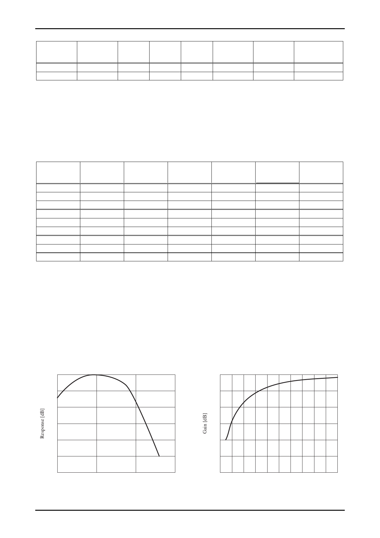
(2) Variable amplifier gain setting
The gain is determined by the value of the resistor (Rg) connected between pin 19 and ground.
Note that the range of values that may be used for Rg is from 4.7kΩ (minimum gain) to 100kΩ (maximum gain).
Bandpass Filter Characteristics
0
–5
– 10
– 15
– 20
– 25
– 30
10
100
1000
Frequency [kHz]
10000
Variable Amplifier Gain Characteristics
30
25
20
15
10
5
0
0 10 20 30 40 50 60 70 80 90 100
Pin 19 resistance (=Rg) [kΩ]
No.A0641-11/14
Share Link: 