TDA5153AG Просмотр технического описания (PDF) - Philips Electronics
Номер в каталоге
Компоненты Описание
производитель
TDA5153AG
Philips Electronics

TDA5153AG Datasheet PDF : 28 Pages
| |||
Philips Semiconductors
Pre-amplifier for Hard Disk Drive (HDD)
with MR-read/inductive write heads
Preliminary specification
TDA5153
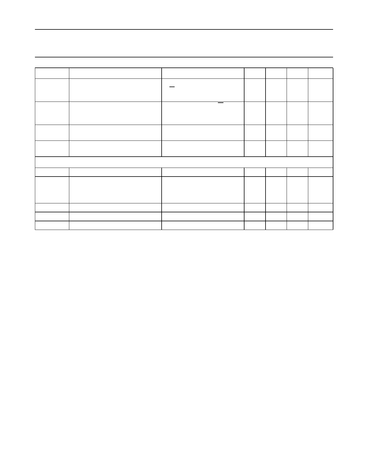
SYMBOL
PARAMETER
tst(W)
write settle times; note 12
toff(W)
write amplifier off time
tsw(W)
tsw(S)
head switching (in write mode),
and standby to write head active
sleep to (and from) any other
modes
DC characteristics
ICC(R)
ICC(W)
supply current; note 13
supply current; note 14
IDD(stb)
IDD(S)
Vref
standby mode supply current
sleep mode supply current
reference voltage for Rext
CONDITIONS
MIN.
from 50%of the falling edge of −
R/W to 90% of the steady state
write current (in Write Mode)
from rising edge of R/W to
−
IWR-programmed /10
(IWR = 35 mA)
from falling edge of SEN to
−
write head active
−
TYP.
−
−
50
−
MAX.
70
50
70
100
UNIT
ns
ns
ns
µs
read mode; IMR = 10 mA
−
72
80
mA
write mode; IWR = 35 mA
from VCC (5 V)
−
33
41
mA
from VCC(WD) (5 to 8 V)
−
54
61
mA
−
0.25 1
mA
static
−
0.025 −
mA
−
1.32 −
V
Notes to the characteristics
1. The differential voltage gain depends on the MR
resistance. It can be improved by programming the
d4 bit in the configuration register using the serial
interface.
2. The gain boost implements a pole-zero combination:
The +3 dB gain boost corner frequency is
--(--8-----⋅---d----3-----+-----4----⋅--8-d--0--2-0----+-M----2-H----⋅-z--d----1-----+----1-----⋅---d----0----)-
The −3 dB gain attenuation corner frequency is
--(--8-----⋅---d----3-----+-----4----⋅--8-d--0--2-0----+-M----2-H----⋅-z--d----1-----+----1-----⋅---d----0----)-
where d3, d2, d1, d0 are bits (0, 1) to be programmed
via the Serial Interface. In practical use, the bandwidth
is limited by the inductance of the connection between
the MR heads and the pre-amplifier.
3. Noise calculation
a) Definitions: The amplifier has a low-ohmic input.
No lead resistance is taken into account. The input
referred noise voltage, excluding the noise of the
MR resistors, is defined as follows:
Vnir2
=
V--G---n-v-o-
2
–
4kT
×
(RMR1 + RMR2)
V
where Gv is the voltage gain and Vno is the noise
voltage at the output of the amplifier, k is the
Boltzmann constant and T is the temperature in K.
The noise figure is defined as follows:
F
=
10
×
log
4----k----T-----×------(--R-----V--GM------n--R-v-o----1----2+-----R----M----R----2---)-
dB
in 1 Hz bandwidth. Note that RMR includes all
resistances between Rx or Ry to ground.
b) Noise figure versus IMR and RMR: Table 1 shows
the variation of the noise figure with IMR (mA) and
RMR (Ω).
c) Input noise voltage consideration: the input
referred noise voltage calculation can significantly
be different (from 1.0 to 0.44 nV/√Hz for instance)
by taking into account an equivalent
signal-to-noise ratio when using two MR stripes
(28 Ω for each stripe) or one MR stripes (42 W).
It assumes that the signal coming from the head is
larger for a dual stripe head than for a single stripe
head (50% extra signal for dual stripe head).
4. The channel separation is defined by the ratio of the
gain response of the amplifier using the selected head
H(n) to the gain response of the amplifier using the
adjacent head H(n ±1), Head H(n) being selected.
1997 Jul 02
21
Share Link: