HT9201B Просмотр технического описания (PDF) - Holtek Semiconductor
Номер в каталоге
Компоненты Описание
производитель
HT9201B Datasheet PDF : 7 Pages
| |||
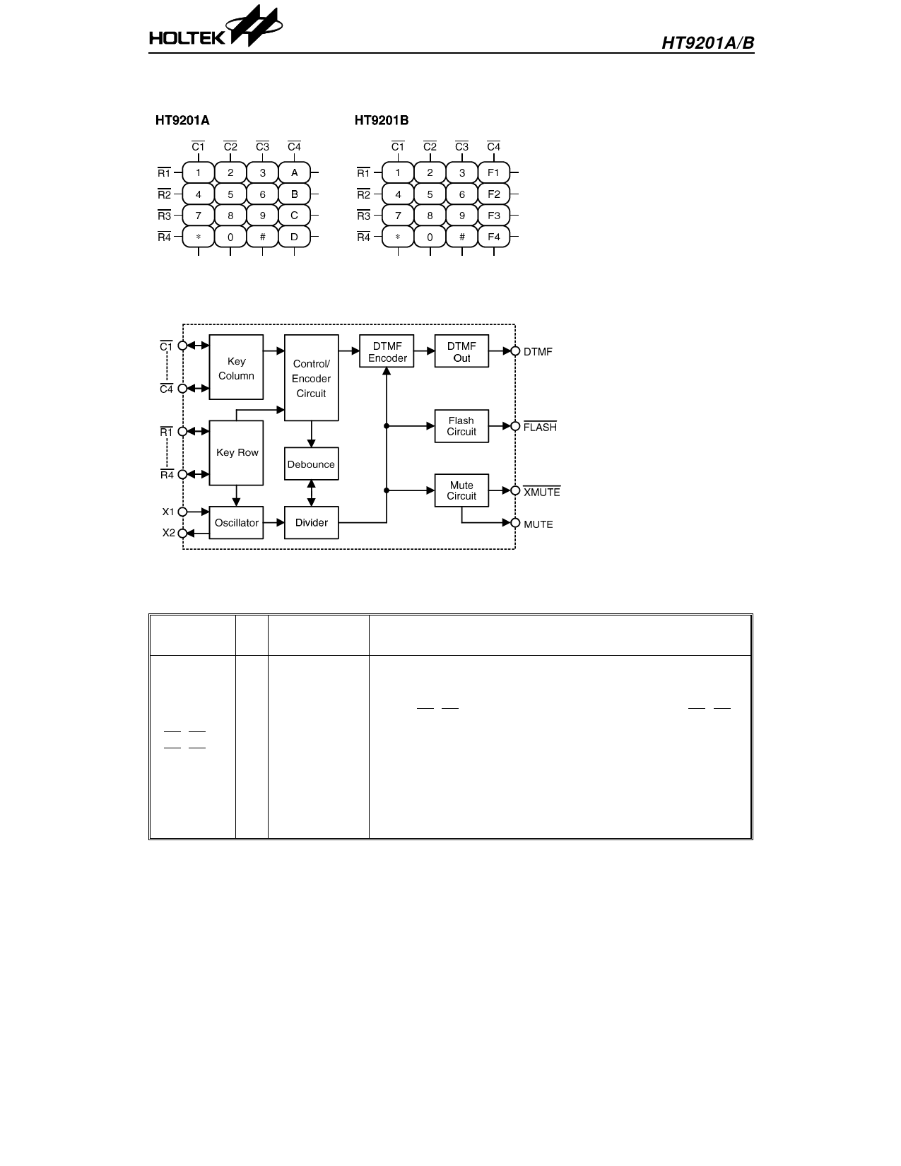
Keyboard Information
Block Diagram
HT9201A/B
Pin Description
Pin Name
I/O
Internal
Connection
Description
C1~C4
R1~R4
These pins form a 4×4 keyboard matrix which can perform
keyboard input detection and dialing specification setting
functions. When the chip is in the standby mode the column
group (C1~C4) remains low whereas the row group (R1~R4) is
I/O
CMOS
IN/OUT
set high for key input detection.
An inexpensive single contact 4×4 keyboard can be used as an
input device. Pressing a key connects a single column to a
single row, and actuates the system oscillator which result in
a dialing signal output. If more than two keys are pressed at a
time, no response occurs. The key-in debounce time is 20ms.
Refer to the keyboard information for keyboard arrangement.
2
3rd Dec ’97
Share Link: 