EVB71122A-868-FSK-A Просмотр технического описания (PDF) - Melexis Microelectronic Systems
Номер в каталоге
Компоненты Описание
производитель
EVB71122A-868-FSK-A
Melexis Microelectronic Systems

EVB71122A-868-FSK-A Datasheet PDF : 32 Pages
| |||
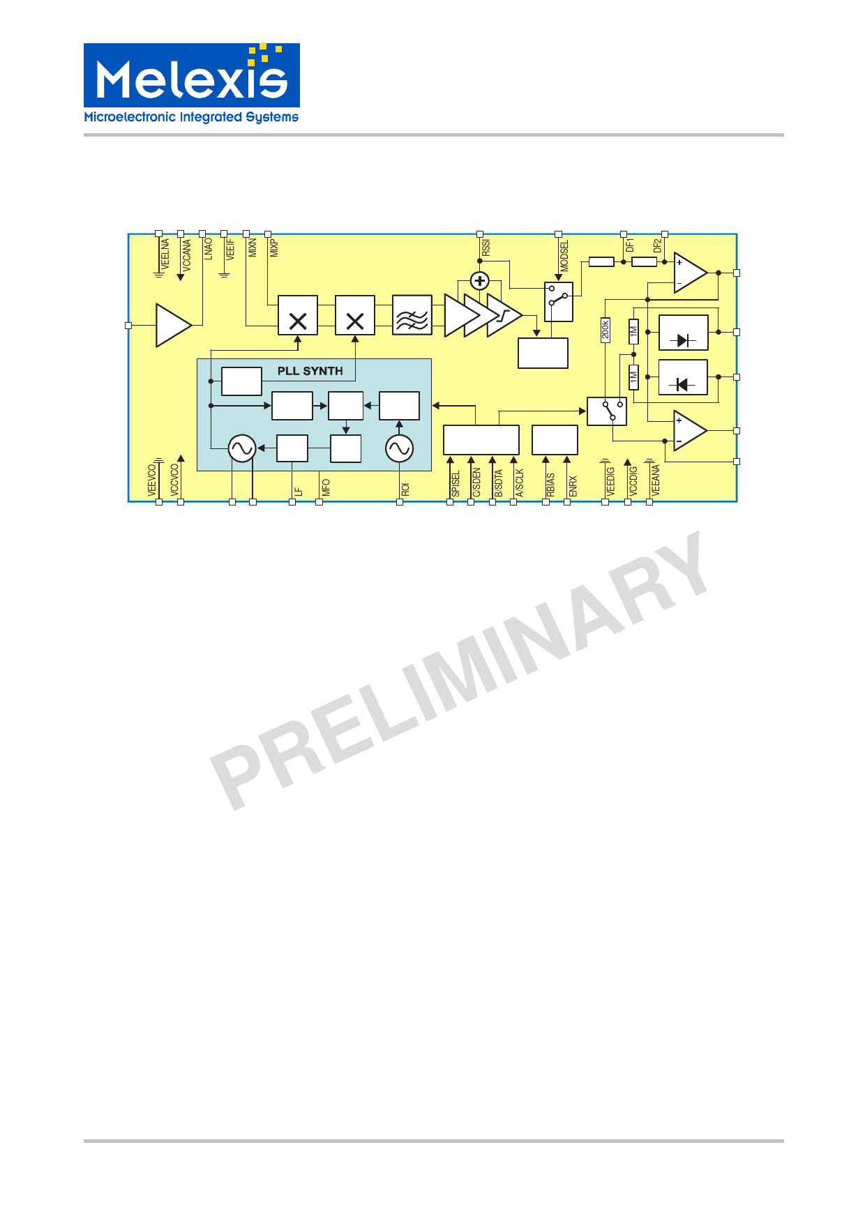
1.3 Block Diagram
EVB71122
300 to 930MHz Receiver
Evaluation Board Description
123456
LNAI LNA
31
MIX1
MIX2
IFF
IF1
IF2
LO1
LO2
LO2DIV
VCO
N/A
counter
LF
PFD
R
counter
CP RO
11 14 TNK1 12 13 TNK2 15 23
24
8
IFA
Control
Logic
9
28
29
200k
200k
DFO
OA1
ASK
27
FSK
SW1
FSK
DEMOD
PKDET+ 25
PDP
PKDET_ PDN
26
SLCSEL
SW2
BIAS
OA2
DTAO
22
SLC
32
7 17 18 19
10 16
20 21 30
Fig. 1: MLX71122 block diagram
PRELIMINARY The MLX71122 receiver IC consists of the following building blocks:
• PLL synthesizer (PLL SYNTH) to generate the first and second local oscillator signals LO1 and LO2,
parts of the PLL SYNTH are the voltage-controlled oscillator (VCO), the feedback dividers N/A and R,
the phase-frequency detector (PFD), the charge pump (CP) and the crystal-based reference oscillator
(RO)
• Low-noise amplifier (LNA) for high-sensitivity RF signal reception
• First mixer (MIX1) for down-conversion of the RF signal to the first IF (intermediate frequency)
• Second mixer (MIX2) with image rejection for down-conversion from the first to the second IF
• IF Filter (IFF) with a 2MHz center frequency and a 230kHz 3dB bandwidth
• IF amplifier (IFA) to provide a large amount of voltage gain and an RSSI signal output
• FSK demodulator (FSK DEMOD)
• Operational amplifiers OA1 and OA2 for low-pass filtering and data slicing, respectively
• Positive (PKDET+) and negative (PKDET-) peak detectors
• Switches SW1 to select between FSK and ASK as well as SW2 to chose between averaging or peak
detector data slicer
• Control logic with 3-wire bus serial programming interface (SPI)
• Biasing circuit with modes control
For more detailed information, please refer to the latest MLX71122 data sheet revision.
39012 71122 01
Rev. 001
Page 5 of 32
EVB Description
Sept/06
Share Link: