ESD11A5.0DT5G Просмотр технического описания (PDF) - ON Semiconductor
Номер в каталоге
Компоненты Описание
производитель
ESD11A5.0DT5G Datasheet PDF : 5 Pages
| |||
ESD11A3.3DT5G SERIES
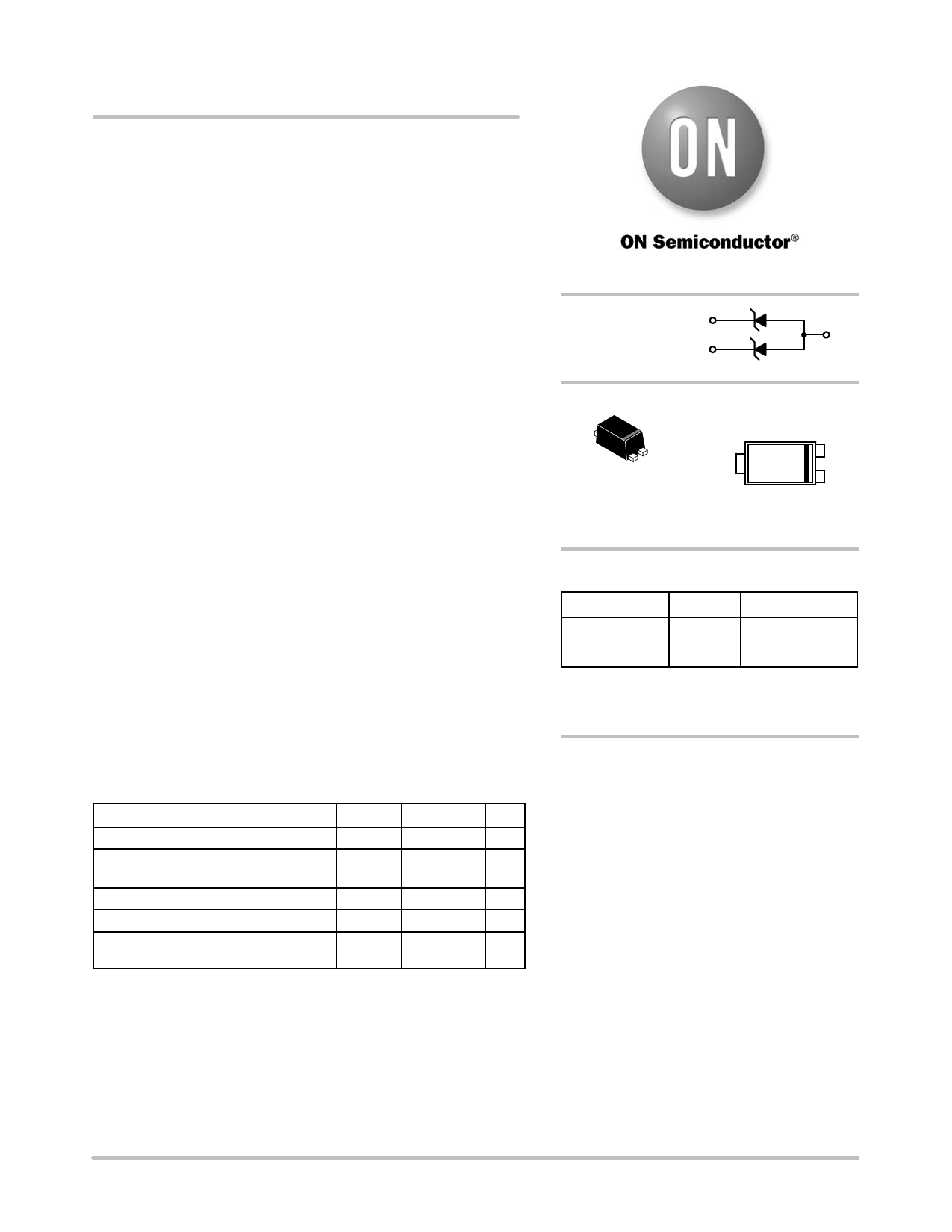
ESD Protection Diode
Ultra Small SOT−1123 Package
The ESD11A Series is designed to protect voltage sensitive
components from damage due to ESD. These parts provide excellent
ESD clamping capability and fast response time to enhance the
immunity of the end application from system level ESD stress such as
IEC61000−4−2. Two uni−directional surge protection diodes are housed
in the ultra small SOT−1123 package, making these parts ideal for ESD
protection on designs where board space is at a premium, such as cell
phones, MP3 players and many other portable handheld electronic
devices.
Specification Features:
• Low Clamping Voltage
• Small Body Outline Dimensions:
0.039” x 0.024” (1.0 mm x 0.6 mm)
• Low Body Height: 0.016″ (0.4 mm)
• Stand−off Voltage: 3.3 V − 5 V
• Low Leakage
• Response Time is Typically < 1 ns
• IEC61000−4−2 Level 4 ESD Protection
• AEC−Q101 Qualified and PPAP Capable
• These are Pb−Free Devices
Mechanical Characteristics:
CASE: Void-free, transfer-molded, thermosetting plastic
Epoxy Meets UL 94 V−0
LEAD FINISH: 100% Matte Sn (Tin)
MOUNTING POSITION: Any
QUALIFIED MAX REFLOW TEMPERATURE: 260°C
Device Meets MSL 1 Requirements
Table 1. MAXIMUM RATINGS
www.onsemi.com
PIN 1. CATHODE 1
2. CATHODE
3
3. ANODE
2
MARKING
DIAGRAM
SOT−1123
CASE 524AA
XM
X = Specific Device Code
M = Date Code
ORDERING INFORMATION
Device
Package
Shipping†
ESD11AxxDT5G SOT−1123 8000/Tape & Reel
(Pb−Free)
†For information on tape and reel specifications,
including part orientation and tape sizes, please
refer to our Tape and Reel Packaging Specifications
Brochure, BRD8011/D.
DEVICE MARKING INFORMATION
See specific marking information in the device marking
column of the table on page 2 of this data sheet.
Rating
Symbol
Value
Unit
IEC 61000−4−2 (ESD)
Contact
Total Power Dissipation on FR−5 Board
(Note 1) @ TA = 25°C
Storage Temperature Range
Junction Temperature Range
Lead Solder Temperature − Maximum
(10 Second Duration)
°PD°
Tstg
TJ
TL
±15
kV
150
mW
−55 to +150 °C
−55 to +125 °C
260
°C
Stresses exceeding those listed in the Maximum Ratings table may damage the
device. If any of these limits are exceeded, device functionality should not be
assumed, damage may occur and reliability may be affected.
1. FR−5 = 1.0 x 0.75 x 0.62 in.
See Application Note AND8308/D for further description of ESD maximum ratings.
© Semiconductor Components Industries, LLC, 2013
1
March, 2019 − Rev. 5
Publication Order Number:
ESD11A3.3D/D
Share Link: 