EM78P5842 Просмотр технического описания (PDF) - ELAN Microelectronics
Номер в каталоге
Компоненты Описание
производитель
EM78P5842 Datasheet PDF : 48 Pages
| |||
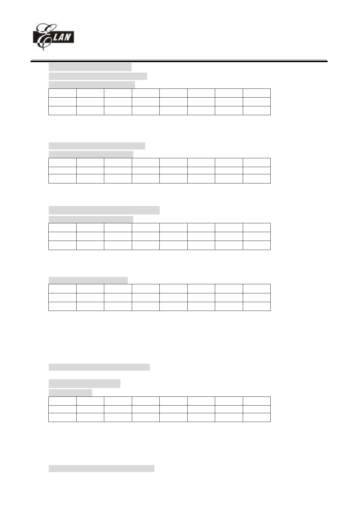
EM78P5840/5841/5842
8-bit Micro-controller
RB (ADC input data buffer)
PAGE0 : (undefined) not allowed to use
PAGE1 (ADC output data register)
7
6
5
4
3
2
1
0
AD7 AD6 AD5 AD4 AD3 AD2 AD1 AD0
R
R
R
R
R
R
R
R
Bit 0 ~ Bit 7 (AD0 ~ AD7) : The last significant 8 bit of 10-bit or whole of 8 bit resolution ADC conversion
output data. Combine there 8 bits and R7 PAGE1 bit4~5 as complete 10-bit ADC conversion output data in 10
bit resolution mode.
PAGE 2 (undefined) not allowed to use
PAGE3 (PRD2: Period of PWM2)
7
6
5
4
3
2
1
0
PRD2[7] PRD2[6] PRD2[5] PRD2[4] PRD2[3] PRD2[2] PRD2[1] PRD2[0]
R/W-0 R/W-0 R/W-0 R/W-0 R/W-0 R/W-0 R/W-0 R/W-0
The content of this register is a period (time base) of PWM2. The frequency of PWM2 is the reverse of the
period.
RC (PORTC I/O data, Counter1 data)
PAGE0 (PORT9 I/O data register)
7
6
5
4
3
2
1
0
X
X
X
X
X
PC2
PC1
X
-
-
-
-
-
R/W
R/W
-
Bit 1 ~ Bit 2 (PC1 ~ PC2) : PORTC1,PORTC2 I/O data register
User can use IOC register to define input or output each bit.
Bit 0; Bit 3~Bit 7: (undefined) not allowed to use.(These bits are not sure to 0 or 1 )
PAGE1 (Counter1 data register)
Bit7
Bit6
Bit5
Bit4
Bit3
Bit2
Bit1
Bit0
CN17 CN16 CN15 CN14 CN13 CN12 CN11 CN10
R/W-0 R/W-0 R/W-0 R/W-0 R/W-0 R/W-0 R/W-0 R/W-0
Bit 0 ~ Bit 7 (CN10 ~ CN17) : Counter1's buffer that user can read and write.
Counter1 is a 8-bit up-counter with 8-bit prescaler that user can use RC PAGE1 to preset and read the
counter.(write Î preset) After a interruption , it will reload the preset value.
Example for writing :
MOV 0x0C, A ; write the data at accumulator to counter1 (preset)
Example for reading :
MOV A, 0x0C ; read the data at counter1 to accumulator
PAGE2,3 (undefined) not allowed to use.
RD (Undefined register)
PAGE0 (Unused)
7
6
5
4
3
2
1
0
X
0
0
0
X
0
0
0
-
R/W-0 R/W-0 R/W-0
-
R/W
R/W
R/W
Bit 0 ~Bit 2 : These three bits must clear to 0 or MCU power consumption will increase.
Bit 3 , Bit 7 : (undefined) not allowed to use
Bit4 ~ Bit6 : These 3 bits are unused in mask/OTP EM785840, but they are used for ICE5830. About the
definition of these 3 bits, please refer to appendix II. In ICE5830, please clear bit4, bit5 and bit6 to 0.
PAGE1,2,3 (undefined) not allowed to use.
__________________________________________________________________________________________________________________________________________________________________
* This specification is subject to change without notice.
15
2004/11/10 V2.6
Share Link: 